
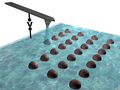
Patterning by Etching at the nanoscale (PENs) is a soft lithographic technique in which the bonds in the polydimethylsiloxane (PDMS) matrix are broken...
2 KB (252 words) - 23:49, 16 May 2022

MEMS (section Etching processes)
deposition of material layers, patterning by photolithography and etching to produce the required shapes. Silicon Silicon is the material used to create most...
45 KB (5,603 words) - 02:57, 3 June 2025

printing Multilayer soft lithography Nanosphere lithography Patterning by etching at the nanoscale Soft lithography has some unique advantages over other forms...
4 KB (368 words) - 16:15, 25 May 2025
traditional subtracting technique like etching. The scale of the structures can vary from the nanoscale up to the centimeter scale or further, but are typically...
5 KB (692 words) - 16:13, 7 January 2025

Nanotechnology (redirect from Nanoscale)
Nanotechnology is the manipulation of matter with at least one dimension sized from 1 to 100 nanometers (nm). At this scale, commonly known as the nanoscale, surface...
71 KB (7,194 words) - 15:34, 24 June 2025
Copper interconnects (section Patterning)
electromigration than Al. Noteworthy, in the case of Al interconnects was patterning process involves selective Al etching (i.e. subtractive manufacturing process)...
11 KB (1,557 words) - 13:09, 15 May 2025

photolithographic patterning. Finally, the individual microcircuits are separated by wafer dicing and packaged as an integrated circuit. In the semiconductor...
37 KB (4,082 words) - 07:16, 16 June 2025
to protect selected areas of it during subsequent etching, deposition, or implantation operations. The term is normally used for processes that can reliably...
3 KB (347 words) - 00:21, 6 January 2025
Lam Research (category Companies in the Nasdaq-100)
while he was at Hewlett Packard that he saw the need for better plasma etching equipment, to keep up with the rapid miniaturization of semiconductor wafers...
21 KB (2,013 words) - 11:59, 6 April 2025

Microfabrication (section Patterning)
scale and the patterning technology is what defines microfabrication. This patterning technique typically uses a 'mask' to define portions of the film which...
20 KB (2,111 words) - 03:31, 25 May 2025
dealing with the engineering (patterning e.g. etching, depositing, writing, printing etc) of nanometer-scale structures on various materials. The modern term...
15 KB (1,678 words) - 10:55, 5 June 2025

example, the soft lithography method, microcontact printing (μCP), is the current standard for low cost, bench-top micro and nanoscale patterning, so it...
22 KB (2,562 words) - 06:44, 25 May 2025

Nanorobotics (section "Swallowing the Surgeon")
To be more precise at a nanoscale, the 3D printing process uses a laser etching machine, which etches the details needed for the segments of nanorobots...
63 KB (7,287 words) - 09:49, 3 June 2025
Local oxidation nanolithography (section Patterning)
for nanoscale-controlled positioning and/or manipulation of those molecules. The patterning of the Mn12 molecules on a silicon surface is achieved by first...
16 KB (1,512 words) - 17:02, 5 January 2025
(2023). "Diversity of dynamic voltage patterns in neuronal dendrites revealed by nanopipette electrophysiology". Nanoscale. doi:10.1039/D2NR03475A. PMC 10373629...
3 KB (299 words) - 13:55, 10 December 2024
procedure that uses highly reactive nanoscale multilayer systems as an intermediate layer between the bonding substrates. The multilayer system consists of...
11 KB (1,245 words) - 20:05, 30 December 2024
Focused ion beam (section Etching)
Because of the sputtering capability, the FIB is used as a micro- and nano-machining tool, to modify or machine materials at the micro- and nanoscale. FIB micro...
26 KB (3,276 words) - 21:51, 19 June 2025

Lithography for nanoscale surface structures and quantum dots Micropatterning of thin films The unique characteristics of micro or nanoscale fluid flow are...
22 KB (2,481 words) - 15:21, 24 May 2025
Probe tip (section Fabrication through etching)
in the nanoscale dimension. This problem can be resolved by taking images of the tip multiple times, followed by combining them into an image by confocal...
72 KB (8,212 words) - 13:26, 17 August 2024

Michel; Duerig, Urs; Knoll, Armin W. (2010). "Nanoscale Three-Dimensional Patterning of Molecular Resists by Scanning Probes". Science. 328 (5979): 732–735...
17 KB (1,822 words) - 04:39, 20 August 2024

substrate material, often by etching. The primary advantage of electron-beam lithography is that it can draw custom patterns (direct-write) with sub-10 nm...
38 KB (4,736 words) - 02:29, 26 May 2025
Evelyn Hu (category Scientists at Bell Labs)
nanofabrication has included high-resolution patterning and high-resolution etching of circuits onto nanoscale materials. She has also developed biological...
8 KB (693 words) - 01:24, 7 May 2025
ablation, etching and others. Nanomanufacturing differs from molecular manufacturing, which is the manufacture of complex, nanoscale structures by means of...
13 KB (1,435 words) - 19:49, 27 May 2025
Cardinal, T; Videau, J. J; Richardson, M; Canioni, L (2010). "3D Patterning at the Nanoscale of Fluorescent Emitters in Glass". Journal of Physical Chemistry...
35 KB (4,269 words) - 18:00, 18 June 2025
Nanosensor (section Chemical etching)
Nanosensors are nanoscale devices that measure physical quantities and convert these to signals that can be detected and analyzed. There are several ways...
50 KB (6,114 words) - 17:47, 23 June 2025
for generating single-layer hexagonally close packed or similar patterns of nanoscale features on nanospheres. Generally, NSL applies planar ordered arrays...
14 KB (1,562 words) - 20:02, 25 May 2025

sub-discipline of the chemical and material sciences that deals with the development of new methods for creating nanoscale materials. The term "nanochemistry"...
39 KB (4,458 words) - 11:18, 26 June 2025

while the less common one, lonsdaleite, has a hexagonal lattice. By mixing these polytypes at the nanoscale, DLC coatings can be made that at the same...
31 KB (4,148 words) - 00:41, 15 June 2025
surface patterning, and microstructuring. A multitude of surface reactions within this context have been explored including metal deposition, etching and...
42 KB (5,218 words) - 01:25, 26 May 2025
Nanolithography is the process of etching, writing or printing structures in the range of nanometer. Small amounts of fluids can be dispensed via the tip of a probe...
8 KB (1,177 words) - 08:17, 31 May 2025