
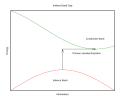
In solid-state physics, the valence band and conduction band are the bands closest to the Fermi level, and thus determine the electrical conductivity of...
6 KB (701 words) - 22:00, 18 July 2025

the conduction band in insulators and semiconductors. It is the energy required to promote an electron from the valence band to the conduction band. The...
26 KB (2,787 words) - 22:12, 16 July 2025
electric charge Valence electron, as an outer shell electron that is associated with an atom Valence and conduction bands, as a conduction band electron relative...
778 bytes (139 words) - 12:54, 17 January 2021
gap". The band gap is called "direct" if the crystal momentum of electrons and holes is the same in both the conduction band and the valence band; an electron...
11 KB (1,578 words) - 20:42, 13 January 2025
of a cell. It introduces an intermediate band (IB) energy level in between the valence and conduction bands. Theoretically, introducing an IB allows two...
17 KB (1,766 words) - 05:54, 30 June 2025
much smaller or nonexistent band gap than semiconductors since the valence and conduction bands overlap. Controlling the band gap allows for the creation...
7 KB (873 words) - 23:01, 27 May 2025

lutetium is primary, sharing both valence electron count and valence orbital type. As chemical reactions involve the valence electrons, elements with similar...
251 KB (27,123 words) - 20:02, 11 July 2025
the trap to the valence or conduction band is much larger than the characteristic thermal energy kT, where k is the Boltzmann constant and T is the temperature...
2 KB (232 words) - 18:46, 20 June 2024
bottom of the conduction band and the top of the valence band, but they do not overlap in momentum space. According to electronic band theory, solids...
9 KB (1,097 words) - 08:53, 2 April 2025
inside of one or more allowed bands. In semimetals the bands are usually referred to as "conduction band" or "valence band" depending on whether the charge...
37 KB (4,835 words) - 08:26, 6 July 2025

OLED (section Manufacturers and commercial uses)
(HOMO and LUMO) of organic semiconductors are analogous to the valence and conduction bands of inorganic semiconductors. Originally, the most basic polymer...
160 KB (17,886 words) - 10:19, 18 July 2025

electron per atom in this model, the valence band is fully occupied, while the conduction band is vacant. The two bands touch at the zone corners (the K point...
269 KB (28,209 words) - 17:10, 19 July 2025
Silicon (section Physical and atomic)
conduction band). The Fermi level is about halfway between the valence and conduction bands and is the energy at which a state is as likely to be occupied...
90 KB (10,922 words) - 17:35, 18 July 2025
greater than that of the intrinsic semiconductor and lies closer to the conduction band than the valence band. Examples: phosphorus, arsenic, antimony, etc...
11 KB (1,231 words) - 16:43, 10 June 2025
Quasi Fermi level (category Electronic band structures)
each band, the conduction band and valence band can each have an individual population that is internally in equilibrium, even though the bands are not...
6 KB (1,052 words) - 21:56, 29 June 2024
Electrons are in the conduction band and holes in the valence band. The electrons that have been excited to the conduction band may become entrapped in...
5 KB (675 words) - 18:14, 15 July 2024
interactions between charge carriers. Valence and conduction bands split slightly compared to the difference between the various bands. Some mechanisms that allow...
2 KB (152 words) - 07:02, 21 February 2025

Electric current (redirect from Electric conduction)
in the conduction band, the band immediately above the valence band. The ease of exciting electrons in the semiconductor from the valence band to the...
36 KB (4,349 words) - 13:25, 13 July 2025

Solar cell (section Intermediate band)
of a cell. It introduces an intermediate band (IB) energy level in between the valence and conduction bands. Theoretically, introducing an IB allows two...
148 KB (16,501 words) - 13:16, 21 July 2025

an energy close to the valence band of the material and those with none have an energy that is closer to the conduction band. In order to gain enough...
25 KB (3,300 words) - 19:59, 17 July 2025
matrix elements shown in the bracket. For the initial and final states in valence and conduction bands, we have | i ⟩ = Ψ v , k i , s i ( r ) {\displaystyle...
31 KB (3,948 words) - 21:13, 1 April 2025

Dirac cone (category Electronic band structures)
materials, at energies near the Fermi level, the valence band and conduction band take the shape of the upper and lower halves of a conical surface, meeting...
23 KB (1,889 words) - 09:38, 22 May 2025

Moss–Burstein effect (category Electronic band structures)
nominally doped semiconductors, the Fermi level lies between the conduction and valence bands. For example, in n-doped semiconductor, as the doping concentration...
3 KB (365 words) - 02:52, 25 May 2025
of the semiconductor and therefore preventing any band bending of the conduction and valence band. An application of the flat band potential can be found...
5 KB (659 words) - 22:00, 17 July 2025

emission, which occurs if the surface energy bands of a semiconductor fall between its valence and conduction bands, which produces a phenomenon known as Fermi...
4 KB (408 words) - 16:34, 17 June 2025

Electron hole (redirect from Hole conduction)
theorem, and demonstrated that a nearly full and a nearly empty Brillouin zones give the opposite Hall voltages. Hole conduction in a valence band can be...
18 KB (2,315 words) - 08:29, 24 June 2025

Bonding molecular orbital Valence and conduction bands Valence bond theory Molecular orbital theory Conjugated system Atkins P. and de Paula J. Atkins Physical...
7 KB (880 words) - 16:28, 11 November 2024

Topological insulator (section Two-band Hamiltonians)
exists an energy gap between the valence and conduction bands of the material. But in a topological insulator, these bands are, in an informal sense, "twisted"...
77 KB (9,290 words) - 14:21, 19 July 2025
Free electron model (category Electronic band structures)
narrow conduction bands also exist. This diversity is not predicted by the model and can only by explained by analysing the valence and conduction bands. Additionally...
24 KB (3,426 words) - 17:10, 29 March 2025
the band gap. It is shifted up for n-doped semiconductors (closer to the conduction band) and down in case of p-doping (nearing the valence band). In...
19 KB (2,686 words) - 15:37, 23 July 2025