The Intel Core microarchitecture (provisionally referred to as Next Generation Micro-architecture, and developed as Merom) is a multi-core processor microarchitecture...
58 KB (3,524 words) - 05:40, 6 August 2025

The P6 microarchitecture is the sixth-generation Intel x86 microarchitecture, first implemented in the Pentium Pro microprocessor in 1995. It was planned...
15 KB (1,526 words) - 05:51, 6 August 2025
the Core microarchitecture. The single- and dual-core models are single-die, whereas the quad-core models comprise two dies, each containing two cores, packaged...
17 KB (1,159 words) - 05:40, 6 August 2025
is the codename for Intel's 45 nm microarchitecture released in November 2008. It was used in the first generation of the Intel Core i5 and i7 processors...
33 KB (1,526 words) - 05:48, 6 August 2025
Intel Core is a line of multi-core (with the exception of Core Solo and Core 2 Solo) central processing units (CPUs) for midrange, embedded, workstation...
280 KB (10,112 words) - 05:40, 6 August 2025
about Intel Turbo Boost Max Technology 3.0". Intel.com. Intel. Retrieved 2020-06-16. "Intel Turbo Boost Technology in Intel Core Microarchitecture (Nehalem)...
9 KB (936 words) - 05:40, 6 August 2025
Gracemont is a microarchitecture for low-power processors used in systems on a chip (SoCs) made by Intel, and is the successor to Tremont. Like its predecessor...
10 KB (426 words) - 05:37, 6 August 2025
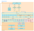
following is a partial list of Intel CPU microarchitectures. The list is incomplete, additional details can be found in Intel's tick–tock model,...
55 KB (3,035 words) - 05:44, 6 August 2025
introduced with the Sandy Bridge CPU microarchitecture on 9 January 2011 and has been found on the die of Intel CPUs ever since. The name "Quick Sync"...
25 KB (1,962 words) - 05:40, 6 August 2025

Intel's codename for its sixth generation Core microprocessor family that was launched on August 5, 2015, succeeding the Broadwell microarchitecture....
103 KB (5,005 words) - 05:57, 6 August 2025
list of Intel Core processors. This includes Intel's original Core (Solo/Duo) mobile series based on the Enhanced Pentium M microarchitecture, as well...
497 KB (14,119 words) - 05:44, 6 August 2025

of the Intel Core processor. It is Intel's codename for the 14 nanometer die shrink of its Haswell microarchitecture. It is a "tick" in Intel's tick–tock...
62 KB (3,129 words) - 05:30, 6 August 2025
fabricated using Intel's 10 nm process node. The microarchitecture is implemented in 10th-generation Intel Core processors for mobile (codenamed Ice Lake) and...
15 KB (1,113 words) - 05:58, 6 August 2025

the Intel Processor brand in 2023. Based on P5 Steppings: B1, C1, D1 (Note: D1 stepping processors do not have FDIV bug) Based on P5 microarchitecture Steppings:...
101 KB (3,933 words) - 04:34, 30 July 2025

the P6 microarchitecture. Its successor, the Core 2 family, was released on July 27, 2006. This was based on the Intel Core microarchitecture, and was...
273 KB (25,488 words) - 05:39, 6 August 2025

In 2006, Intel announced a plan to return the Pentium trademark from retirement to the market, as a moniker of low-cost Core microarchitecture processors...
11 KB (1,021 words) - 06:55, 3 August 2025
instruction set used in the Intel Core microarchitecture and AMD K10 (K8L). It was announced on September 27, 2006, at the Fall 2006 Intel Developer Forum, with...
23 KB (1,613 words) - 15:39, 30 July 2025

Haswell is the codename for a processor microarchitecture developed by Intel as the "fourth-generation core" successor to the Ivy Bridge (which is a die...
113 KB (5,142 words) - 05:37, 6 August 2025
through emulation. These are based on the Intel Xe-LP microarchitecture, the low power variant of the Intel Xe GPU architecture also known as Gen 12....
83 KB (4,723 words) - 05:40, 6 August 2025
NetBurst (redirect from Intel NetBurst (microarchitecture))
The NetBurst microarchitecture, called P68 inside Intel, was the successor to the P6 microarchitecture in the x86 family of central processing units (CPUs)...
16 KB (1,656 words) - 05:48, 6 August 2025

(Celeron, 64-bit Core microarchitecture) – 65 nm process technology Variants Intel Celeron E1600, 2.40 GHz (512 KB L2, 800 MHz FSB) Intel Celeron E1500,...
205 KB (13,785 words) - 05:44, 6 August 2025

Pentium 4 (redirect from Intel Pentium 4)
Intel shifted development away from NetBurst to focus on the cooler-running Pentium M microarchitecture. On January 5, 2006, Intel launched the Core processors...
46 KB (5,423 words) - 05:51, 6 August 2025
Pentium (redirect from Intel Pentium)
flagship processor line for over a decade until the introduction of the Intel Core line in 2006. Pentium-branded processors released from 2009 onwards were...
41 KB (2,656 words) - 03:44, 30 July 2025
Bridge is the codename for Intel's 22 nm microarchitecture used in the third generation of the Intel Core processors (Core i7, i5, i3). Ivy Bridge is...
66 KB (2,736 words) - 05:41, 6 August 2025
Based on Core microarchitecture Chip harvests from Conroe with half L2 cache disabled All models support: MMX, SSE, SSE2, SSE3, SSSE3, Intel 64, XD bit...
44 KB (877 words) - 10:18, 25 July 2024

LGA 771 (category Intel CPU sockets)
Intel in 2006. It is used in Intel Core microarchitecture and NetBurst microarchitecture (Dempsey) based DP-capable server processors, the Dual-Core Xeon...
8 KB (367 words) - 14:27, 12 May 2025

Sandy Bridge (redirect from Intel Sandy Bridge (microarchitecture))
for Intel's 32 nm microarchitecture used in the second generation of the Intel Core processors (Core i7, i5, i3). The Sandy Bridge microarchitecture is...
63 KB (2,744 words) - 05:56, 6 August 2025
Bonnell is a CPU microarchitecture used by Intel Atom processors which can execute up to two instructions per cycle. Like many other x86 microprocessors...
27 KB (2,482 words) - 05:30, 6 August 2025
process and supports up to 24 cores. It includes the Intel Gen11 graphics architecture from Ice Lake. Tremont microarchitecture provides the following enhancements...
17 KB (542 words) - 06:00, 6 August 2025
Pentium (original) (redirect from Intel P5 (microarchitecture))
succeeding the i486, its implementation and microarchitecture was internally called P5. Like the Intel i486, the Pentium is instruction set compatible...
40 KB (3,903 words) - 05:52, 6 August 2025