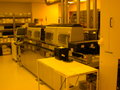
Atomic layer etching (ALE) is an emerging technique in semiconductor manufacture, in which a sequence alternating between self-limiting chemical modification...
2 KB (223 words) - 20:33, 23 August 2023
Atomic layer deposition (ALD) is a thin-film deposition technique based on the sequential use of a gas-phase chemical process; it is a subclass of chemical...
65 KB (7,443 words) - 09:49, 30 June 2025
Semiconductor device fabrication (section Metal layers)
conductivity) Etching (microfabrication) Dry etching (plasma etching) Reactive-ion etching (RIE) Deep reactive-ion etching (DRIE) Atomic layer etching (ALE) Plasma...
112 KB (11,789 words) - 11:25, 15 July 2025
aspect ratio structures. The company uses reactive ion etch (RIE) and atomic layer etching (ALE) to shape a variety of conductive and dielectric features. The...
21 KB (2,013 words) - 11:59, 6 April 2025
Asymptotically locally Euclidean, a division of gravitational instanton Atomic layer etching, a technique in semiconductor device fabrication Automatic link establishment...
3 KB (384 words) - 07:00, 29 April 2025
Joseph, Eric A.; Oehrlein, Gottlieb S. (2014). "Fluorocarbon assisted atomic layer etching of SiO2 using cyclic Ar/C4F8 plasma". Journal of Vacuum Science &...
4 KB (274 words) - 20:39, 13 June 2025
sodium etching is defluorination of the PTFE, stripping the fluorine molecules from the carbon backbone of the polymer. The fluorine-to-carbon atomic ratio...
14 KB (1,883 words) - 09:08, 8 February 2025
semiconductor manufacturers in fabrication plants for processes such as atomic layer deposition, epitaxy, chemical vapor deposition, and diffusion. The company...
18 KB (1,767 words) - 10:27, 28 May 2025
MXenes prepared via HF etching have an accordion-like morphology, which can be referred to as multi-layer MXene (ML-MXene), or few-layer MXene (FL-MXene) given...
76 KB (8,630 words) - 12:01, 19 July 2025

MEMS (section Etching processes)
the basic techniques are deposition of material layers, patterning by photolithography and etching to produce the required shapes. Silicon Silicon is...
45 KB (5,603 words) - 02:57, 3 June 2025

Ion beam (redirect from Ion beam etching)
modification (e.g. by sputtering or ion beam etching) and for ion beam analysis. Ion beam application, etching, or sputtering, is a technique conceptually...
9 KB (1,097 words) - 06:31, 8 April 2025
manner. Essentially, MLD resembles the well established technique of atomic layer deposition (ALD) but, whereas ALD is limited to exclusively inorganic...
65 KB (8,543 words) - 00:26, 6 July 2025

fluorocarbon etching of silicon in an inductively coupled plasma: Mechanism of etching through a thick steady state fluorocarbon layer Archived 2016-02-07...
7 KB (879 words) - 03:53, 21 July 2025
prevention steps are applied. The oxide layer removal can be realized by various oxide etch chemistry methods. Dry etching processes, i.e. formic acid vapor...
13 KB (1,465 words) - 09:17, 28 May 2024
deposition (MOCVD), wet wafer processing, molecular beam epitaxy (MBE), atomic layer deposition (ALD), physical vapor deposition (PVD), dicing and lapping...
19 KB (1,924 words) - 22:04, 18 July 2025

composition across the surface, or in depth profiling when paired with ion-beam etching. It is often applied to study chemical processes in the materials in their...
43 KB (6,279 words) - 10:25, 27 June 2025

bonding Reactive ion etching Tommi Kääriäinen; David Cameron; Marja-Leena Kääriäinen; Arthur Sherman (17 May 2013). Atomic Layer Deposition: Principles...
1 KB (103 words) - 18:14, 26 November 2023
Black silicon (section Reactive-ion etching)
ion etching (RIE). Other methods for forming a similar structure include electrochemical etching, stain etching, metal-assisted chemical etching, and...
32 KB (3,246 words) - 18:04, 22 May 2025

Epitaxy (redirect from Epitaxial layer)
source gas, liberated by evaporation or wet etching of the surface, may also diffuse into the epitaxial layer and cause autodoping. The concentration of...
30 KB (3,623 words) - 22:20, 23 July 2025

Sputtering (section Etching and chemical sputtering)
to act on extremely fine layers of material is utilised in science and industry—there, it is used to perform precise etching, carry out analytical techniques...
27 KB (3,315 words) - 19:43, 29 July 2025
wafer processing steps from the creation of metal interconnect layers through the final etching step that creates pad openings (see also front end of line...
14 KB (1,689 words) - 01:32, 27 July 2025
scientist known for her research developing advanced atomic layer deposition (ALD) and etching techniques. Her research focuses on creating thin films...
7 KB (594 words) - 17:35, 21 November 2024

clean silicon. To remove existing native oxide layers wet chemical etching (HF clean), dry chemical etching or chemical vapor deposition (CVD) with different...
19 KB (2,052 words) - 08:00, 16 April 2025

surface. Photolithography and etching removes some polymer layers to uncover conductive pads on the ICs. Afterwards, the anode layer is applied to the device...
160 KB (17,886 words) - 10:19, 18 July 2025

Ion track (redirect from Particle track etching)
cross-linking (dominating in the track halo). Low atomic mobility: For selective ion track etching, the density contrast between the latent ion track...
39 KB (4,000 words) - 04:27, 12 September 2024

Spiral groove bearing (section Etching)
This method differs from regular etching as two layers are placed on the surface to be grooved, but only the upper layer is exposed to the etchant, leaving...
14 KB (1,953 words) - 14:14, 10 July 2025
Probe tip (section Fabrication through etching)
single atoms yields specific atomic configuration at the probe tip, which yields very high resolution. Electrochemical etching is one of the most widely...
72 KB (8,212 words) - 13:26, 17 August 2024

few-layer boron nitride sheets have a strength similar to that of monolayer boron nitride. Thermal conductivity. The thermal conductivity of atomically thin...
21 KB (2,357 words) - 22:37, 10 April 2025

microscopy. Atomic force microscope tips can be used as a nanoscale "write head" to deposit a resist, which is then followed by an etching process to remove...
71 KB (7,194 words) - 15:34, 24 June 2025

electron beam. Etching must be done only in the absorbing layer and thus there is a need to distinguish between the capping and the absorbing layer, which is...
126 KB (14,698 words) - 08:12, 31 July 2025