be represented as an immersion minor of its planarization. In incremental planarization, the planarization process is split into two stages. First, a large...
10 KB (1,184 words) - 07:11, 2 June 2023
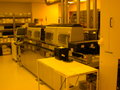
Chemical-mechanical polishing (redirect from Chemical mechanical planarization)
Chemical mechanical polishing (CMP) (also called chemical mechanical planarization) is a process of smoothing surfaces with the combination of chemical...
9 KB (1,331 words) - 01:38, 25 May 2025

Tetrahedral molecular geometry (section Planarization)
In a tetrahedral molecular geometry, a central atom is located at the center with four substituents that are located at the corners of a tetrahedron. The...
11 KB (1,197 words) - 22:53, 24 May 2025

elements: Selecting the type of wafer to be used; Chemical-mechanical planarization (CMP) and cleaning of the wafer. Shallow trench isolation (STI) (or...
6 KB (661 words) - 07:11, 3 June 2025
Inc. is an American company that manufactures chemical-mechanical planarization slurries, ultra-thin dielectric and metal precursors of film, formulated...
3 KB (136 words) - 17:30, 22 October 2021
rate based on an increased surface contact. Also the use of an ultra planarization step is considered to improve the bonding due to a reduction of material...
13 KB (1,465 words) - 09:17, 28 May 2024

industries. In 2006 it was reported being used in electrochemical–mechanical planarization of copper layers in the semiconductor devices fabrication process. Reduction...
44 KB (4,097 words) - 20:02, 1 June 2025
to pattern. CMP (chemical-mechanical planarization) is the primary processing method to achieve such planarization, although dry etch back is still sometimes...
113 KB (11,851 words) - 15:31, 13 June 2025
including photolithography, wet etch and clean, chemical-mechanical planarization, thin-film deposition, bulk chemical processing, wafer and reticle handling...
6 KB (548 words) - 11:23, 7 March 2025

polymers and photoresists can result in relatively large edge beads whose planarization has physical limits. Cohen, Edward; Lightfoot, E. J. (2011). "Coating...
7 KB (852 words) - 18:14, 30 March 2025

fiberglass, inks, and inkjet paper, and in the chemical-mechanical planarization process as an emulsifier and disintegrant for solution polymerization...
20 KB (2,124 words) - 11:12, 15 June 2025
chip equipment manufacturer that specialized in chemical-mechanical planarization (CMP) cleaning, for $225 million. CMP cleaning is a hybrid process to...
21 KB (2,013 words) - 11:59, 6 April 2025

Virtual detail of an integrated circuit through four layers of planarized copper interconnect, down to the polysilicon (pink), wells (greyish), and substrate...
86 KB (9,193 words) - 19:37, 22 May 2025

1990s, including chemical-mechanical polishing or chemical mechanical planarization (CMP), trench isolation, and copper interconnects—although not directly...
104 KB (10,706 words) - 19:42, 14 June 2025

market, packaging coatings and increasing use of chemical mechanical planarization (CMP). While MEMS manufacturing continues to be dominated by used semiconductor...
45 KB (5,603 words) - 02:57, 3 June 2025
edges of the wafer or photomask with increased resist thickness whose planarization has physical limits. Often, Edge bead removal (EBR) is carried out,...
59 KB (6,439 words) - 19:14, 23 May 2025

by either thermal diffusion or ion implantation Chemical-mechanical planarization (CMP) Wafer cleaning, also known as "surface preparation" (see below)...
20 KB (2,111 words) - 03:31, 25 May 2025

the excess dielectric using a technique such as chemical-mechanical planarization. Certain semiconductor fabrication technologies also include deep trench...
5 KB (522 words) - 23:01, 14 February 2025

processing, including doping, lithography, patterning, deposition, planarization, etching, and cleaning. After the acquisition of Intermolecular, its...
48 KB (4,805 words) - 19:51, 11 June 2025
temperature. The viscous flow of glass has effects to compensate and planarize surface irregularities, convenient for bonding wafers with a high roughness...
24 KB (2,970 words) - 10:23, 24 May 2025
wafer in trichloroethylene, acetone and methanol. Chemical-mechanical planarization Piranha solution Plasma etching Silicon on insulator Wafer (electronics)...
6 KB (721 words) - 22:57, 7 November 2024
Combinatorial map a combinatorial object that can encode plane graphs Planarization, a planar graph formed from a drawing with crossings by replacing each...
35 KB (4,541 words) - 18:29, 29 May 2025

Krishnan, Jakub W. Nalaskowsk, and Lee M. Cook, "Chemical Mechanical Planarization: Slurry Chemistry, Materials, and Mechanisms" Chem. Rev., 2010, vol...
9 KB (962 words) - 04:46, 18 April 2025

application of ceria is for polishing, especially chemical-mechanical planarization (CMP). In its other main application, CeO2 is used to decolorize glass...
51 KB (6,075 words) - 02:18, 15 June 2025
different out-of-plane bending and dihedral torsion parameters in order to planarize delocalized trigonal nitrogen atoms, e.g. in aniline. The "s" in MMFF94s...
2 KB (255 words) - 22:15, 17 July 2023

difficult to produce. Atomic layer deposition (ALD) Chemical-mechanical planarization (CMP) Chemical vapor deposition (CVD) Crystalline silicon Ion implantation...
25 KB (2,776 words) - 14:13, 23 May 2025
District, Migdal HaEmek 0.235 1989, 1986 150 1000–350 14,000 Foundry, Planarized BEOL, W and Oxide CMP, CMOS, CIS, Power, Power Discrete Tower Semiconductor...
209 KB (6,859 words) - 16:09, 5 June 2025
the trenches is deposited on the insulator, and chemical-mechanical planarization (CMP) is used to remove the copper (known as overburden) that extends...
11 KB (1,557 words) - 13:09, 15 May 2025

in which an input graph is planarized by replacing crossing points by vertices, a topological embedding of the planarized graph is found, edge orientations...
31 KB (3,275 words) - 10:55, 8 May 2025
polishing, a technique used in semiconductor fabrication; also known as planarization Command Module Pilot, a position of the Apollo program crewed missions...
3 KB (447 words) - 16:09, 16 June 2025