Plasma etching is a form of plasma processing used to fabricate integrated circuits. It involves a high-speed stream of glow discharge (plasma) of an appropriate...
16 KB (1,860 words) - 19:04, 29 March 2025

etchants are liquid-phase ("wet") and plasma-phase ("dry"). Each of these exists in several varieties. The first etching processes used liquid-phase ("wet")...
17 KB (1,558 words) - 09:49, 28 May 2024
strength. The primary methods currently used in industry are sodium etching and plasma etching. Results of ion beam treatment and laser surface roughening have...
14 KB (1,883 words) - 09:08, 8 February 2025

MEMS (section Etching processes)
wet etching, and use plasma etching instead. Plasma etchers can operate in several modes by adjusting the parameters of the plasma. Ordinary plasma etching...
45 KB (5,603 words) - 20:43, 20 March 2025

response of plasma to electromagnetic fields is used in many modern devices and technologies, such as plasma televisions or plasma etching. Depending on...
62 KB (6,405 words) - 01:53, 22 February 2025

Reactive-ion etching (RIE) is an etching technology used in microfabrication. RIE is a type of dry etching which has different characteristics than wet etching. RIE...
6 KB (724 words) - 03:59, 27 June 2024
techniques include: Plasma activation Plasma ashing Plasma cleaning Plasma electrolytic oxidation Plasma etching Plasma functionalization Plasma polymerization...
1 KB (96 words) - 11:56, 30 December 2023
residues by oxygen plasmas is sometimes correctly described as a dry etch process. The term plasma ashing can be used instead. Dry etching is particularly...
6 KB (678 words) - 05:26, 19 October 2023

Fluorochemical industry (section Plasma etching)
thin metal films onto semiconductors. Tetrafluoromethane, is used for plasma etching in semiconductor manufacturing, flat panel display production, and...
37 KB (3,685 words) - 03:37, 8 August 2024
sputtering, plasma-enhanced chemical vapor deposition (PECVD)) and etching. Inductively coupled plasma Multipactor effect Plasma etching UK Wireless Telegraphy...
3 KB (384 words) - 19:36, 15 February 2025
representing the available ionic species. Plasma etching Plasma Processing: Proceedings of the Symposium on Plasma Processing. Electrochemical Society. 1987...
3 KB (476 words) - 10:22, 25 April 2023
three categories: Plasma etching systems (RIE, ICP, DRIE) Plasma deposition systems (PECVD and LS-CVD®) Surface treatment systems (plasma cleaners, UV-Ozone...
4 KB (270 words) - 13:55, 8 February 2024
used today is called plasma etching. Plasma etching usually involves an etch gas pumped in a low-pressure chamber to create plasma. A common etch gas is...
47 KB (5,524 words) - 20:32, 22 April 2025
Lam Research (section Plasma etch)
was while he was at Hewlett Packard that he saw the need for better plasma etching equipment, to keep up with the rapid miniaturization of semiconductor...
21 KB (2,013 words) - 11:59, 6 April 2025
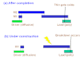
each net is disconnected from the initial global metal layer, and the plasma etching is still adding charges to each piece of metal. Leaky gate oxides, although...
8 KB (1,097 words) - 15:34, 19 December 2024

Marshall's acid (H2S2O8) Peroxymonosulfuric acid, or Caro's acid (H2SO5) Plasma etching RCA clean (silicon wafer cleaning procedure) Superhydrophilicity Ultrahydrophobicity...
20 KB (2,214 words) - 12:01, 6 May 2025
from MIT, Lam worked on plasma etching research and engineering at Texas Instruments and Hewlett-Packard. Although plasma etching was widely used in R&D...
15 KB (1,542 words) - 19:13, 2 February 2025
easily by oxygen, fluorine, chlorine and other reactive gases used in plasma etching. Use of a hardmask involves an additional deposition process, and hence...
3 KB (356 words) - 08:29, 16 July 2022

Chemical milling (redirect from Industrial etching)
desired shape. Other names for chemical etching include photo etching, chemical etching, photo chemical etching and photochemical machining. It is mostly...
12 KB (1,532 words) - 00:36, 25 April 2025

coupled plasma Induction plasma technology Pulsed inductive thruster High density fluorocarbon etching of silicon in an inductively coupled plasma: Mechanism...
7 KB (879 words) - 11:48, 8 April 2025
both make use of helicons in their plasma heating phase). Helicons are also utilized in the procedure of plasma etching, used in the manufacture of computer...
8 KB (1,170 words) - 11:33, 20 January 2024
Dry etching (plasma etching) Reactive-ion etching (RIE) Deep reactive-ion etching (DRIE) Atomic layer etching (ALE) Plasma ALE Thermal ALE Wet etching Buffered...
110 KB (11,624 words) - 05:45, 5 May 2025

Microfabrication (section Etching)
removed. Etching techniques include: Dry etching (plasma etching) such as reactive-ion etching (RIE) or deep reactive-ion etching (DRIE) Wet etching or chemical...
20 KB (2,111 words) - 23:59, 6 March 2025
in liquid-, gas- or plasma-phase, although liquid etchants such as buffered hydrofluoric acid (BHF) for silicon dioxide etching are more often used....
2 KB (193 words) - 21:16, 18 September 2024
Photolithography (section Etching, implantation)
durable protecting layer in future ion implantation, wet chemical etching, or plasma etching. From preparation until this step, the photolithography procedure...
59 KB (6,439 words) - 05:12, 3 May 2025

Printed circuit board manufacturing (section Etching)
through, this smear must be removed by a chemical de-smear process, or by Plasma etching. The de-smear process ensures that a good connection is made to the...
35 KB (4,567 words) - 01:10, 7 March 2025
time-multiplexed etching, alternates repeatedly between two modes to achieve nearly vertical structures: A standard, nearly isotropic plasma etch. The plasma contains...
13 KB (1,454 words) - 15:24, 28 February 2025

shareholder in the company. Naura has four business lines: Semiconductors (plasma etching, PVD, CVD, oxidation/diffusion, cleaning system, and annealing) Vacuum...
14 KB (1,158 words) - 06:38, 26 April 2025

Research in Shanghai alleging infringement of trade secrets related to plasma etching equipment. In March 2017, the court sided in favour of AMEC but Lam...
11 KB (1,044 words) - 06:02, 25 April 2025
usually carried out by chemical etching of the covering, laser cutting, laser evaporation of the covering, plasma etching or mechanical removal of the cover...
8 KB (726 words) - 04:39, 4 February 2025