Atomic layer deposition (ALD) is a thin-film deposition technique based on the sequential use of a gas-phase chemical process; it is a subclass of chemical...
65 KB (7,440 words) - 04:51, 17 February 2025
Atomic layer epitaxy (ALE), more generally known as atomic layer deposition (ALD), is a specialized form of thin film growth (epitaxy) that typically...
5 KB (568 words) - 18:07, 5 May 2021
Essentially, MLD resembles the well established technique of atomic layer deposition (ALD) but, whereas ALD is limited to exclusively inorganic coatings...
65 KB (8,538 words) - 12:35, 23 May 2025

of. CVD is extremely useful in the process of atomic layer deposition at depositing extremely thin layers of material. A variety of applications for such...
42 KB (5,024 words) - 16:41, 21 May 2025
(2014-12-01). "A Short History of Atomic Layer Deposition: Tuomo Suntola's Atomic Layer Epitaxy". Chemical Vapor Deposition. 20 (10–11–12): 332–344. doi:10...
2 KB (223 words) - 20:33, 23 August 2023
Thin film (redirect from Thin-film deposition)
Many growth methods rely on nucleation control such as atomic-layer epitaxy (atomic layer deposition). Nucleation can be modeled by characterizing surface...
66 KB (8,526 words) - 13:29, 22 May 2025
in fabrication plants for processes such as atomic layer deposition, epitaxy, chemical vapor deposition, and diffusion. The company was founded by Arthur...
18 KB (1,767 words) - 10:27, 28 May 2025
reactions underpinning the thin film deposition technique that years later became known as atomic layer deposition. He was the rector of Leningrad Technological...
8 KB (696 words) - 20:47, 16 November 2024

a thin film is a prerequisite and the preferred growth mode is atomic layer deposition, Al2O3 films can be prepared by the chemical exchange between trimethylaluminium...
38 KB (3,774 words) - 05:15, 23 May 2025
trenches. The requisite layers, an anode, separator, and cathode, for a battery were then added by low-pressure chemical vapor deposition. The battery consists...
23 KB (2,752 words) - 22:24, 11 February 2025
Substrate (chemistry) (section Atomic layer deposition)
interest in diffraction patterns by differentiating by phase. In atomic layer deposition, the substrate acts as an initial surface on which reagents can...
14 KB (1,617 words) - 22:15, 29 May 2025
etch and deposition, metal organic chemical vapor deposition (MOCVD), wet wafer processing, molecular beam epitaxy (MBE), atomic layer deposition (ALD),...
19 KB (1,922 words) - 15:04, 26 August 2024
evaporation (e.g. CrBO3, β-BaB2O4), pulsed laser deposition (e.g. β-BaB2O4, Eu(BO2)3), and atomic layer deposition (ALD). Growth by ALD was achieved using precursors...
24 KB (2,658 words) - 16:15, 25 May 2025

materials science, developing the thin film growth technique called atomic layer deposition. Suntola was born in Tampere, Pirkanmaa, in 1943, during the Continuation...
10 KB (1,174 words) - 01:50, 31 May 2025
Nanolamination (section Atomic layer deposition)
created using atomic layer deposition (ALD) with unique physical, chemical, and electronic properties. For example, a rough oxide layer can be further...
5 KB (560 words) - 22:11, 16 May 2024

Pulsed laser deposition (PLD) is a physical vapor deposition (PVD) technique where a high-power pulsed laser beam is focused inside a vacuum chamber to...
21 KB (2,603 words) - 02:05, 28 December 2024
Deposition can be viewed as a reverse process to dissolution or particle re-entrainment. Atomic layer deposition Chemical vapor deposition Deposition...
2 KB (217 words) - 00:57, 27 May 2025

Optical rectenna (section Atomic layer deposition)
University of Connecticut are using a technique called selective area atomic layer deposition that is capable of producing them reliably and at industrial scales...
29 KB (3,668 words) - 03:32, 26 May 2025
Lam Research (section Thin film deposition)
electrochemical deposition (ECD) and chemical vapor deposition (CVD) technologies to form copper and other metal films for conducting structures. Atomic layer deposition...
21 KB (2,013 words) - 11:59, 6 April 2025
be created using both synthetic and natural polymer materials. Atomic layer deposition (ALD) is a vapor-phase technique used to produce films with high...
22 KB (2,357 words) - 06:20, 29 May 2025
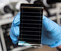
Perovskite solar cell (section Deposition methods)
TiO2 layer deposition be compatible with flexible polymer substrate, low-temperature techniques, such as atomic layer deposition, molecular layer deposition...
200 KB (22,835 words) - 01:39, 23 May 2025

focused ion beam machining, nanoimprint lithography, atomic layer deposition, and molecular vapor deposition, and further including molecular self-assembly...
71 KB (7,194 words) - 18:10, 30 April 2025
Semiconductor device fabrication (section Metal layers)
(CVD) Metal organic chemical vapor deposition (MOCVD), used in LEDs Atomic layer deposition (ALD) Physical vapor deposition (PVD) Sputtering Evaporation Epitaxy...
113 KB (11,784 words) - 00:35, 25 May 2025
Layer-by-layer (LbL) deposition is a thin film fabrication technique. The films are formed by depositing alternating layers of complementary materials...
9 KB (1,082 words) - 04:02, 17 March 2025
computers." The IEEE states: "Sandhu initiated the development of atomic layer deposition high-κ films for DRAM devices and helped drive cost-effective implementation...
5 KB (406 words) - 03:43, 31 July 2024
required for transformation of a substance, or completion of the alchemical magnum opus. Atomic layer deposition Mond process Thermal decomposition v t e...
750 bytes (77 words) - 05:05, 12 February 2025
Assistive listening device used to improve hearing ability Atomic layer deposition, a thin-film deposition technique Asymmetric Laplace distribution, in probability...
2 KB (257 words) - 21:17, 8 May 2023

using inkjet printing, and the inorganic layers are applied using Atomic Layer Deposition (ALD). The encapsulation process is carried out under a nitrogen...
159 KB (17,822 words) - 18:14, 27 May 2025

chemical vapor deposition or atomic layer deposition. The Al2O3 provides excellent surface passivation of p-doped silicon surfaces. The Al2O3 layer is typically...
11 KB (920 words) - 14:10, 23 May 2025

electroluminescent material is deposited using atomic layer deposition, which is a process that deposits one 1-atom thick layer at a time. EL works by exciting atoms...
4 KB (481 words) - 13:47, 15 May 2025