
A chip scale package or chip-scale package (CSP) is a type of integrated circuit package. Originally, CSP was the acronym for chip-size packaging. Since...
3 KB (370 words) - 22:06, 25 August 2023

standard J-STD-012, Implementation of Flip Chip and Chip Scale Technology, in order to qualify as chip scale, the package must have an area no greater than 1...
62 KB (3,442 words) - 15:44, 29 May 2025

Integrated circuit (redirect from Computer chip)
"Startup shrinks Peltier cooler, puts it in the chip package". 10 January 2008. "Wire Bond Vs. Flip Chip Packaging | Semiconductor Digest". 10 December 2016...
86 KB (9,193 words) - 19:37, 22 May 2025

before the packaging components are attached. WLP is essentially a true chip-scale package (CSP) technology, since the resulting package is practically...
6 KB (724 words) - 23:58, 25 October 2024

package technologies that connect ICs to the surfaces of PCBs without through-holes. Flat no-lead is a near chip scale plastic encapsulated package made...
15 KB (1,875 words) - 07:37, 21 January 2025
Ball Grid Array PSfcCSP: refers to the bottom package: Package Stackable Flip Chip Chip Scale Package In 2001, a Toshiba research team including T. Imoto...
13 KB (1,373 words) - 09:31, 26 January 2025

technology Surface-mount technology Chip carrier Pin grid array Flat package Small Outline Integrated Circuit Chip-scale package Ball grid array Transistor, diode...
15 KB (1,590 words) - 06:50, 22 April 2025

Hershey Company. During the fall season from 2016 to 2023 the chip was sold in various packaging before being declared "sold out". The challenge was tried...
25 KB (2,290 words) - 22:21, 9 May 2025
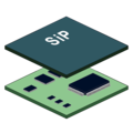
in a package (SiP) or system-in-package is a number of integrated circuits (ICs) enclosed in one chip carrier package or encompassing an IC package substrate...
10 KB (1,143 words) - 14:17, 25 May 2025
Solder ball (redirect from Package ball)
array, chip-scale package, and flip chip packages generally use solder balls. After the solder balls are used to attach an integrated circuit chip to a...
3 KB (268 words) - 21:52, 27 January 2025

flip chip interconnects (in particular copper pillar solder bumps) for use in electronics and optoelectronic packaging, including: flip chip packaging of...
20 KB (2,779 words) - 18:36, 2 February 2025

(components per hour), using standard PCB assembly equipment. Flip chip packages often consist of a silicon die sitting on top of a "substrate" which...
16 KB (1,777 words) - 09:34, 20 March 2025

Semiconductor device fabrication (redirect from Silicon chip fabrication)
however, Flip-chip packaging can be used to place bond pads across the entire surface of the die. Chip scale package (CSP) is another packaging technology...
113 KB (11,851 words) - 15:31, 13 June 2025
Three-dimensional integrated circuit (redirect from Chip bonding)
Designs of Stack Chip Scale Package". Retrieved 2014-05-15.[permanent dead link] "High Density PoP (Package-on-Package) and Package Stacking Development"...
81 KB (8,790 words) - 20:07, 4 June 2025
The packaging services include fan-out wafer-level packaging (FO-WLP), wafer-level chip-scale packaging (WL-CSP), flip chip, 2.5D and 3D packaging, system...
12 KB (1,275 words) - 00:01, 15 April 2025

A chip scale atomic clock (CSAC) is a compact, low-power atomic clock fabricated using techniques of microelectromechanical systems (MEMS) and incorporating...
8 KB (902 words) - 00:36, 20 October 2024

could be put on a DIP package, leading to development of higher-density chip carriers. Furthermore, square and rectangular packages made it easier to route...
23 KB (3,294 words) - 23:17, 31 January 2025

accelerometer for the iPhone and created the company's first wafer level chip scale package for inertial sensor. He is a player in the U.S. semiconductor industry...
7 KB (547 words) - 08:09, 21 April 2025

(embedded) of an integrated circuit package like BGA or CSP (chip scale package) substrate or interposer of packages. electronic designs which require numerous...
22 KB (2,387 words) - 23:32, 23 May 2025

LPDDR, and flash storage chips, such as eUFS or eMMC, which may be stacked directly on top of the SoC in a package-on-package (PoP) configuration or placed...
43 KB (4,739 words) - 20:02, 17 June 2025

components on the same printed circuit board (PCB). A package related to QFP is plastic leaded chip carrier (PLCC) which is similar but has pins with larger...
10 KB (1,190 words) - 13:50, 13 June 2025

ARM Cortex-M (section Chips)
the Cortex-M0+ type (as of 2014, smallest at 1.6 mm by 2 mm in a chip-scale package is Kinetis KL03). On 21 June 2018, the "world's smallest computer'"...
82 KB (5,908 words) - 20:35, 26 May 2025

Pin grid array (redirect from Flip-chip pin grid array)
flip chip mounting. Typically, PGA packages use wire bonding when the chip is mounted on the pinned side, and flip chip construction when the chip is on...
10 KB (967 words) - 16:44, 20 November 2024
and statistical data analysis Carriage service provider Chip-scale package, or chip-size package Client-side prediction, a network programming technique...
4 KB (456 words) - 23:49, 26 March 2025
footprint areas (e.g. flip-chip packages, chip-scale packages, and direct chip attachments), and on the printed circuit board and package substrate level, to...
10 KB (1,351 words) - 21:21, 27 April 2025

General Instrument AY-3-8910 (redirect from AY chip)
package of the same name. The AY-3-8912 is the same chip in a 28-pin package, with parallel port B simply not connected to any pins. Smaller packages...
16 KB (2,220 words) - 02:24, 15 June 2025
recognized the ink dot. For today's multi-die packages such as stacked chip-scale package (SCSP) or system in package (SiP) – the development of non-contact...
5 KB (727 words) - 23:22, 10 December 2024
Association, United States association Polymer Stud Grid Array, a chip scale package This disambiguation page lists articles associated with the title...
237 bytes (59 words) - 08:23, 29 April 2020
transactions at full bandwidth Point-to-point data interconnect Chip scale package packaging Dynamic request scheduling Early-read-after-write support for...
17 KB (1,896 words) - 15:27, 13 August 2024
Wafer-scale integration (WSI) is a system of building very-large integrated circuit (commonly called a "chip") networks from an entire silicon wafer to...
10 KB (1,283 words) - 15:38, 28 February 2025