Scanning gate microscopy (SGM) is a scanning probe microscopy technique with an electrically conductive tip used as a movable gate that couples capacitively...
2 KB (244 words) - 21:39, 16 March 2022
Scanning voltage microscopy (SVM), sometimes also called nanopotentiometry, is a scientific experimental technique based on atomic force microscopy. A...
4 KB (456 words) - 03:28, 11 September 2024
Scanning probe microscopy (SPM) is a branch of microscopy that forms images of surfaces using a physical probe that scans the specimen. SPM was founded...
29 KB (3,378 words) - 04:36, 25 March 2025
Scanning quantum dot microscopy (SQDM) is a scanning probe microscopy (SPM) that is used to image nanoscale electric potential distributions on surfaces...
12 KB (1,600 words) - 12:02, 19 February 2025

Kelvin probe force microscope (redirect from Kelvin probe microscopy)
force microscopy (KPFM), also known as surface potential microscopy, is a noncontact variant of atomic force microscopy (AFM). By raster scanning in the...
34 KB (4,279 words) - 14:55, 11 May 2025
of Variable Temperature Setup for Scanning Electron Microscopy in Gases and Liquids at Ambient Conditions. Microscopy and Microanalysis 21 (3),765-770...
8 KB (1,232 words) - 20:08, 26 October 2024
Scanning capacitance microscopy (SCM) is a variety of scanning probe microscopy in which a narrow probe electrode is positioned in contact or close proximity...
7 KB (892 words) - 07:17, 25 March 2023
near-field (photon-tunneling microscopy as well as those that use the Pendry Superlens and near field scanning optical microscopy) or on the far-field. Among...
89 KB (10,346 words) - 03:04, 14 April 2025

Transmission electron microscopy (TEM) is a microscopy technique in which a beam of electrons is transmitted through a specimen to form an image. The specimen...
118 KB (15,039 words) - 04:49, 18 May 2025

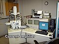
preamplifier for the current) is a strong advantage compared to scanning tunneling microscopy (STM). Basically, in STM the topography picture is constructed...
50 KB (5,994 words) - 09:40, 15 April 2025

The environmental scanning electron microscope (ESEM) is a scanning electron microscope (SEM) that allows for the option of collecting electron micrographs...
69 KB (8,297 words) - 20:15, 8 May 2025
photoelectron spectroscopy (PES), transmission electron microscopy (TEM), and scanning electron microscopy (SEM). In 1933, Ernst Brüche reported images of cathodes...
20 KB (2,699 words) - 21:36, 26 September 2024

times faster than those offered by point-scanning methods. This method is used in cell biology and for microscopy of intact, often chemically cleared, organs...
42 KB (4,675 words) - 12:57, 30 March 2025

Optical coherence tomography (redirect from OCT scan)
information obtained by coherence-gating through an axially scanning reference arm (Fig. 2). Two-dimensional lateral scanning has been electromechanically...
91 KB (10,281 words) - 18:08, 19 March 2025
In microscopy, scanning joule expansion microscopy (SJEM) is a form of scanning probe microscopy heavily based on atomic force microscopy (AFM) that maps...
19 KB (2,760 words) - 05:51, 25 September 2022

Nanotechnology (section Scanning microscopes)
example, feature-oriented scanning approach, atoms or molecules can be moved around on a surface with scanning probe microscopy techniques. Various techniques...
71 KB (7,194 words) - 18:10, 30 April 2025
by simulations as well as experiments at low temperature using scanning gate microscopy. A model with springs and ropes can show that a hung weight can...
27 KB (3,634 words) - 21:21, 2 December 2024

related to microscopy or scanning probe microscopy, instead of the description of nanorobots as molecular machines. Using the microscopy definition,...
63 KB (7,313 words) - 18:36, 15 March 2025

Multi-tip scanning tunneling microscopy (Multi-tip STM) extends scanning tunneling microscopy (STM) from imaging to dedicated electrical measurements...
20 KB (2,169 words) - 21:10, 16 May 2024
Two-photon laser scanning fluorescence microscopy Denk 1994, Proc Natl Acad Sci USA. Two-photon scanning photochemical microscopy: mapping ligand-gated ion channel...
18 KB (1,710 words) - 17:19, 28 November 2023
Second Generation Multiplex DNA profiling system - also see SGM+ Scanning gate microscopy Spherical Grating Monochromator beamline of Canadian Light Source...
2 KB (277 words) - 03:26, 26 October 2023
developed. These are the scanning acoustic microscope (SAM), confocal scanning acoustic microscope (CSAM), and C-mode scanning acoustic microscope (C-SAM)...
19 KB (2,441 words) - 07:56, 23 March 2025
Nanophotonics (section Microscopy)
sharp tips used in near-field scanning optical microscopy (SNOM or NSOM) and photoassisted scanning tunnelling microscopy. Nanophotonics researchers pursue...
24 KB (2,705 words) - 06:05, 3 April 2025

Molybdenum ditelluride (section Microscopy)
laser-induced-metal phase of MoTe2 and its contact property via scanning gate microscopy". Nanotechnology. 31 (20): 205205. arXiv:2001.07860. Bibcode:2020Nanot...
56 KB (6,480 words) - 05:55, 12 April 2025
Schottky barriers in carbon nanotube field-effect transistors via Scanning Gate Microscopy. Johnson has also achieved significant advancements in nanoscale...
16 KB (1,324 words) - 14:23, 21 August 2024
phylum. He has also contributed to the creation of new scanning electron microscopy and light microscopy techniques. Funch has over 170 publications about...
4 KB (222 words) - 06:29, 4 February 2024
imaging, Raman spectroscopy, super resolution microscopy as well as a wide variety of modern fluorescence microscopy techniques thanks to greater SNR in low-light...
50 KB (6,364 words) - 05:15, 23 April 2025
logic gate Nanolithography Moore's law Semiconductor device fabrication Semiconductor scale examples Nanometrology Atomic force microscopy Scanning tunneling...
17 KB (1,965 words) - 16:46, 4 May 2025

(characterization methods such as electron microscopy, X-ray diffraction, calorimetry, nuclear microscopy (HEFIB), Rutherford backscattering, neutron...
64 KB (6,723 words) - 00:28, 2 May 2025
is a semiconductor analysis technique performed in a scanning electron microscope (SEM) or scanning transmission electron microscope (STEM). It is most...
9 KB (1,085 words) - 03:57, 12 May 2024