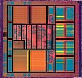
Wafer-scale integration (WSI) is a system of building very-large integrated circuit (commonly called a "chip") networks from an entire silicon wafer to...
10 KB (1,283 words) - 15:38, 28 February 2025

Integrated circuit (redirect from Small-scale integration)
stands for "ultra-large-scale integration" was proposed for chips of more than 1 million transistors. Wafer-scale integration (WSI) is a means of building...
86 KB (9,193 words) - 03:50, 27 April 2025
of integrating all components on a single-crystal silicon wafer, which led to small-scale integration (SSI) in the early 1960s, and then medium-scale integration...
15 KB (1,599 words) - 11:38, 17 April 2025
Ivor Catt (section Wafer scale integration)
College, Cambridge. Catt developed and patented some ideas on Wafer scale integration (WSI) in 1972, and published his work in Wireless World in 1981...
9 KB (997 words) - 20:46, 30 July 2024

chip-scale package (CSP) technology, since the resulting package is practically of the same size as the die. Wafer-level packaging allows integration of...
6 KB (724 words) - 23:58, 25 October 2024
currently part of the Analog MEMS and Sensors business group; in 2000: WaferScale Integration Inc. (WSI, Fremont, California), a vendor of EPROM and flash-memory-based...
39 KB (4,071 words) - 17:06, 1 May 2025

since the communication requirements for the chips are the same. Wafer-scale integration is another possibility. The primary limitations on this method...
6 KB (681 words) - 20:43, 28 February 2025

Technologically these devices are all cryogenic and scaling to large numbers of qubits requires wafer-scale integration, a serious engineering challenge by itself...
113 KB (12,419 words) - 13:17, 14 May 2025
later went to work for a number of startups, including Synertek, Wafer Scale Integration and San Disk. He and Sanjay Mehrotra co-founded SanDisk in 1988...
3 KB (233 words) - 21:49, 26 April 2025

Eclipse. On August 19, 2019, Cerebras announced its first-generation Wafer-Scale Engine (WSE).’ In November 2019, Cerebras closed its series E round with...
39 KB (3,999 words) - 01:02, 11 March 2025
technologies developed by the main company. These included Anamartic Ltd (wafer-scale integration), Shaye Communications Ltd (CT2 mobile telephony) and Cambridge...
31 KB (3,197 words) - 23:59, 15 May 2025
problem by producing all of the circuit boards on a single wafer, known as wafer scale integration (WSI). Instead of making many small boards and wiring them...
9 KB (1,134 words) - 04:06, 16 October 2024

other three-dimensional integrated circuits Multi-chip module WSI (wafer-scale integration) Proximity communication Surface-mount components are usually smaller...
62 KB (3,450 words) - 02:46, 21 January 2025

multi-project wafer (MPW) semiconductor manufacturing arrangements allow customers to share tooling (like mask) and microelectronics wafer fabrication cost...
19 KB (2,030 words) - 08:36, 4 April 2025
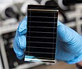
Perovskite solar cell (section Scalability)
sustainable technique for medium scale manufacturing, for instance, for standalone modules or Si wafer-scale integration. This work shows that through judicious...
200 KB (22,835 words) - 04:05, 6 May 2025
general, 3D integration is a broad term that includes such technologies as 3D wafer-level packaging (3DWLP); 2.5D and 3D interposer-based integration; 3D stacked...
81 KB (8,788 words) - 12:09, 10 May 2025
The acronym WSI may refer to: Wafer-scale integration, a technique for building large integrated circuits Wall Street Institute, the former name of Wall...
1 KB (204 words) - 02:36, 17 May 2025

a single wafer of electronic-grade silicon (EGS) or other semiconductor (such as GaAs) through processes such as photolithography. The wafer is cut (diced)...
5 KB (462 words) - 13:05, 1 March 2025
Semiconductor device fabrication (section Wafers)
of wafers from machine to machine. A wafer often has several integrated circuits which are called dies as they are pieces diced from a single wafer. Individual...
111 KB (11,735 words) - 11:17, 12 May 2025
Barsoum, Emad (13 April 2022). "Supporting PyTorch on the Cerebras Wafer-Scale Engine - Cerebras". Cerebras. Retrieved 29 December 2024. Ltd, Graphcore...
5 KB (298 words) - 16:49, 16 January 2025
Very-large-scale integration (VLSI) lithography uses projection systems. Unlike contact or proximity masks, which cover an entire wafer, projection masks...
59 KB (6,439 words) - 11:39, 15 May 2025

The idea of using an entire wafer for a single computer processor was in vogue at the time, see wafer scale integration. The worst-case scenario was...
55 KB (7,776 words) - 19:39, 14 March 2025

technologies developed by the company. These included Anamartic Ltd. (wafer-scale integration) and Cambridge Computer Ltd. (Z88 portable computer and satellite...
45 KB (4,785 words) - 05:56, 13 May 2025
the design, modeling, and applications of multi-chip modules and wafer-scale integration. It was established in 1999 and ceased publication in 2010. The...
2 KB (98 words) - 03:54, 31 July 2024

vertical electrical connection (via) that passes completely through a silicon wafer or die. TSVs are high-performance interconnect techniques used as an alternative...
15 KB (1,733 words) - 13:37, 3 May 2025
they are still part of the wafer wafer-to-wafer (also wafer-on-wafer) stacking – bonding and integrating whole processed wafers atop one another before dicing...
14 KB (1,689 words) - 19:08, 30 December 2024

Etching (microfabrication) (redirect from Wafer etching)
from the surface of a wafer during manufacturing. Etching is a critically important process module in fabrication, and every wafer undergoes many etching...
17 KB (1,558 words) - 09:49, 28 May 2024


18.7, p. 405. Rosenberg, Arnold L. (1986), "Book embeddings and wafer-scale integration", Proceedings of the seventeenth Southeastern international conference...
68 KB (8,167 words) - 00:16, 5 October 2024

of surface micromachining and has realized the co-integration of MEMS and integrated circuits. Wafer bonding involves joining two or more substrates (usually...
45 KB (5,603 words) - 20:43, 20 March 2025