Substrate is a term used in materials science and engineering to describe the base material on which processing is conducted. Surfaces have different...
4 KB (436 words) - 08:49, 25 August 2024

Materials science is an interdisciplinary field of researching and discovering materials. Materials engineering is an engineering field of finding uses...
64 KB (6,723 words) - 00:28, 2 May 2025
chemistry, where the substrate is the chemical of interest that is being modified. In biochemistry, an enzyme substrate is the material upon which an enzyme...
14 KB (1,609 words) - 08:39, 27 March 2025
tiles Substrate (chemistry), the reactant which is consumed during a catalytic or enzymatic reaction Substrate (materials science), the material on which...
2 KB (261 words) - 08:45, 10 December 2024
Stratum (linguistics) (redirect from Substrate Theories)
the prestige of science and of its language). In the case of French, for example, Latin is the superstrate and Gaulish the substrate. Some linguists contend...
32 KB (2,934 words) - 23:33, 2 May 2025
may have contributed the substrate material is an ongoing subject of academic debate and study. The non-Indo-European substrate hypothesis attempts to explain...
22 KB (2,148 words) - 19:12, 15 May 2025
composed of the following materials: M1: Si3N4 M2: Poly-Si M3: Sidewall Oxide (SiO2) M4: SiO2 M5: Si3N4 M6: SiO2 M7: Si Substrate M8: Air Accurate n and...
31 KB (3,368 words) - 22:59, 29 June 2024
Substrate is the earthy material that forms or collects at the bottom of an aquatic habitat. It is made of sediments that may consist of: Silt – A loose...
3 KB (337 words) - 07:13, 27 August 2024
materials and the improvement of existing materials is an important field of study in materials science. Most commonly used semiconductor materials are...
54 KB (2,525 words) - 16:50, 24 May 2025

Enzyme (redirect from Enzyme-substrate complex)
The molecules upon which enzymes may act are called substrates, and the enzyme converts the substrates into different molecules known as products. Almost...
99 KB (10,086 words) - 19:06, 23 May 2025

Wafer (electronics) (redirect from Substrate (electronics))
In electronics, a wafer (also called a slice or substrate) is a thin slice of semiconductor, such as a crystalline silicon (c-Si, silicium), used for...
36 KB (4,088 words) - 14:39, 18 April 2025
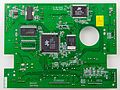
Printed circuit board (redirect from PCB material stack-up)
constant, are gaining importance. The circuit-board substrates are usually dielectric composite materials. The composites contain a matrix (usually an epoxy...
50 KB (6,249 words) - 02:59, 23 May 2025

two-dimensional growth. Here the substrate is the thin-film material. Heteroepitaxy is a kind of epitaxy performed with materials that are different from each...
30 KB (3,624 words) - 17:18, 27 February 2025
Substrate-level phosphorylation is a metabolism reaction that results in the production of ATP or GTP supported by the energy released from another high-energy...
11 KB (1,219 words) - 01:47, 3 November 2024

Surface energy (category Surface science)
detaching of bodies of well defined shape made of one material from the substrate made from the second material. For example, the relative surface energy of the...
33 KB (4,063 words) - 15:27, 29 March 2025
Thin film (category Materials science)
layer of materials ranging from fractions of a nanometer (monolayer) to several micrometers in thickness. The controlled synthesis of materials as thin...
66 KB (8,526 words) - 13:29, 22 May 2025

the material that is to be deposited. This material is vaporized from the target (in a plasma plume) which deposits it as a thin film on a substrate (such...
21 KB (2,603 words) - 02:05, 28 December 2024
Vertically aligned carbon nanotube arrays (category Refractory materials)
In materials science, vertically aligned carbon nanotube arrays (VANTAs) are a unique microstructure consisting of carbon nanotubes oriented with their...
53 KB (7,306 words) - 15:09, 13 May 2025

densities using porous materials, one can increase electric car mileage range. Another use case for nanoporous materials is as a substrate for gas sensors....
14 KB (1,665 words) - 18:39, 22 May 2025

Circuit Boards). Typically, polymers are chosen as substrates or material to embed. When bending the substrate, the outermost radius of the bend will stretch...
14 KB (1,666 words) - 07:21, 5 March 2025

sulphidic substrate Animals moving on / in surface of sea-floor Loose, oxygenated upper substrate with burrowing animals The "Cambrian substrate revolution"...
22 KB (2,594 words) - 20:59, 23 May 2025
Spin methods involve depositing materials onto a spinning substrate. This method is generally used for flat substrates due to inherent limitations of spin...
22 KB (2,357 words) - 00:06, 23 May 2025

high-performance, solid materials. The process is often used in the semiconductor industry to produce thin films. In typical CVD, the wafer (substrate) is exposed...
42 KB (5,024 words) - 16:41, 21 May 2025

gradient). While all materials have a nonzero thermoelectric effect, in most materials it is too small to be useful. However, low-cost materials that have a sufficiently...
116 KB (14,118 words) - 15:03, 22 May 2025
tramways or local railways in Belgium. In materials science, a "vicinal substrate" is a thin-film substrate whose surface normal deviates slightly from...
765 bytes (140 words) - 04:07, 20 April 2025

cells with multiple p–n junctions made of different semiconductor materials. Each material's p–n junction will produce electric current in response to different...
61 KB (8,210 words) - 16:30, 24 May 2025

Ion implantation (category Materials science)
semiconductor device fabrication and in metal finishing, as well as in materials science research. The ions can alter the elemental composition of the target...
39 KB (4,311 words) - 12:03, 13 May 2025

ejecting material from a "target" that is a source onto a "substrate" such as a silicon wafer. Resputtering is re-emission of the deposited material during...
23 KB (2,857 words) - 20:44, 23 May 2025

the source will control the rate of material impinging on the substrate surface and the temperature of the substrate will affect the rate of hopping or...
14 KB (1,527 words) - 07:34, 12 May 2025
Nanocellulose (section Bio-based coloured materials)
family of cellulosic materials that have at least one of their dimensions in the nanoscale. Examples of nanocellulosic materials are microfibrilated cellulose...
75 KB (8,271 words) - 13:00, 23 May 2025