
A p–n junction is a combination of two types of semiconductor materials, p-type and n-type, in a single crystal. The "n" (negative) side contains freely-moving...
19 KB (2,718 words) - 18:54, 12 June 2025
p–n junction isolation is a method used to electrically isolate electronic components, such as transistors, on an integrated circuit (IC) by surrounding...
5 KB (577 words) - 20:59, 17 March 2023
BJTs use two p–n junctions between two semiconductor types, n-type and p-type, which are regions in a single crystal of material. The junctions can be made...
54 KB (6,645 words) - 01:21, 1 June 2025
A p–n diode is a type of semiconductor diode based upon the p–n junction. The diode conducts current in only one direction, and it is made by joining a...
24 KB (3,620 words) - 23:14, 26 August 2024
Depletion region (redirect from Junction voltage)
depletion region forms instantaneously across a p–n junction. It is most easily described when the junction is in thermal equilibrium or in a steady state:...
18 KB (2,589 words) - 18:54, 12 June 2025

example, and particularly, the p–n junction—will receive this energy, and because of the asymmetric response of the junction to an electric field, it will...
5 KB (540 words) - 01:46, 14 December 2024

Diode (redirect from Junction diode)
type today, is a crystalline piece of semiconductor material with a p–n junction connected to two electrical terminals. It has an exponential current–voltage...
64 KB (7,336 words) - 22:38, 28 April 2025
Quasi Fermi level (section p–n junction)
applied to a p–n junction, the quasi Fermi levels for electron and holes overlap with one another. As bias increase, the valence band of the p-side gets...
6 KB (1,052 words) - 21:56, 29 June 2024

Doping (semiconductor) (redirect from N-doping)
the p-n junction's properties are due to the band bending that happens as a result of the necessity to line up the bands in contacting regions of p-type...
40 KB (5,211 words) - 03:21, 23 May 2025
PIN diode (redirect from P-i-n junction)
structure, or p-i-n junction, of a solar cell. In this case, the advantage of using a PIN structure over conventional semiconductor p–n junction is better...
15 KB (2,169 words) - 17:45, 6 May 2025
contact. Electrical junctions types include thermoelectricity junctions, metal–semiconductor junctions and p–n junctions. Junctions are either rectifying...
1 KB (133 words) - 17:43, 22 October 2023

Schottky barrier (redirect from Schottky junction)
mechanism, Schottky diodes can achieve greater switching speeds than p–n junction diodes, making them appropriate to rectify high-frequency signals. Introducing...
16 KB (2,095 words) - 19:42, 20 May 2025

Multi-junction (MJ) solar cells are solar cells with multiple p–n junctions made of different semiconductor materials. Each material's p–n junction will...
61 KB (8,213 words) - 06:26, 3 June 2025
Ohmic contact (redirect from Nonrectifying junction)
a junction or contact that does not demonstrate a linear I–V curve is called non-ohmic. Non-ohmic contacts come in a number of forms, such as p–n junction...
13 KB (1,470 words) - 22:14, 28 December 2022

As with photodiodes and APDs, a SPAD is based around a semi-conductor p-n junction that can be illuminated with ionizing radiation such as gamma, x-rays...
44 KB (6,277 words) - 23:51, 23 May 2025
concentration and regions of p- and n-type dopants. A single semiconductor device crystal can have many p- and n-type regions; the p–n junctions between these regions...
47 KB (5,523 words) - 12:23, 5 June 2025

designed to exploit the voltage-dependent capacitance of a reverse-biased p–n junction. Varactors are used as voltage-controlled capacitors. They are commonly...
12 KB (1,560 words) - 17:54, 21 April 2025
a p-n junction diode, electrons and holes are the minority charge carriers in the p-region and the n-region, respectively. In an unbiased junction, due...
6 KB (806 words) - 21:29, 28 July 2024

its internal junction and diffusion capacitance and reverse recovery time. Shockley derives an equation for the voltage across a p-n junction in a long article...
12 KB (1,866 words) - 09:49, 24 April 2025

positive-to-negative (P-N) junction that is about 10 nm (100 Å) wide. The heavy doping results in a broken band gap, where conduction band electron states on the N-side...
15 KB (1,591 words) - 16:18, 26 May 2025
to electrically isolate components on a semiconductor crystal, using p–n junction isolation. The first monolithic IC chip was invented by Robert Noyce...
74 KB (9,046 words) - 18:56, 14 June 2025

semiconductor. The electron-hole pairs generated by light falling outside the p-n junction are not separated by the electric field, and thus the electron-hole pairs...
52 KB (5,618 words) - 20:03, 4 June 2025
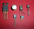
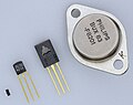
Transistor (section Bipolar junction transistor (BJT))
two p-type semiconductors (a p–n–p transistor). This construction produces two p–n junctions: a base-emitter junction and a base-collector junction, separated...
99 KB (10,298 words) - 23:03, 8 June 2025
are also critical to a full analysis of p-n junction devices such as bipolar junction transistors and p-n junction diodes. The electron–hole pair is the...
27 KB (4,197 words) - 01:56, 26 May 2025
composed of a P-N junction with a wide depletion region, inside which two additional contacts are made: the injector and the modulator. The P material was...
1 KB (167 words) - 05:03, 31 July 2024

p–n junction with a low Zener voltage, in which case the reverse conduction occurs due to electron quantum tunnelling in the short distance between p...
18 KB (2,334 words) - 17:43, 18 April 2025

is the maximum theoretical efficiency of a solar cell using a single p–n junction to collect power from the cell where the only loss mechanism is radiative...
44 KB (6,222 words) - 12:09, 25 May 2025

interface between an n-type (donor doped) and p-type (acceptor doped) semiconductor such as silicon, this is called a p–n junction. This is not a necessary...
2 KB (169 words) - 00:58, 17 March 2025
most common semiconductor device today, is known as a p–n junction.) Metal–semiconductor junctions are crucial to the operation of all semiconductor devices...
23 KB (2,601 words) - 15:14, 23 May 2025

photocells to gamma ray spectrometers. A photodiode is a PIN structure or p–n junction. When a photon of sufficient energy strikes the diode, it creates an...
29 KB (3,387 words) - 18:53, 12 June 2025