
Selected area (electron) diffraction (abbreviated as SAD or SAED) is a crystallographic experimental technique typically performed using a transmission...
15 KB (1,710 words) - 23:20, 13 July 2024
overview of electron diffraction and electron diffraction patterns, collective referred to by the generic name electron diffraction. This includes aspects...
143 KB (15,555 words) - 12:41, 24 June 2025

Brillouin-zone construction by selected area diffraction, using 300 keV electrons....
11 KB (640 words) - 06:31, 24 September 2024
Bragg's law (redirect from Bragg diffraction)
periodic microscale lattices. Bragg diffraction (also referred to as the Bragg formulation of X-ray diffraction) was first proposed by Lawrence Bragg...
23 KB (2,670 words) - 06:34, 2 June 2025

high accuracy. QSTEM can also be applied to selected area diffraction patterns and convergent beam diffraction patterns to quantify the degree and types...
37 KB (4,263 words) - 23:40, 22 May 2025
spectroscopy – Resonance Raman spectroscopy SAD – Selected area diffraction SAED – Selected area electron diffraction SAM – Scanning Auger microscopy SANS – Small...
15 KB (1,398 words) - 20:21, 9 November 2024
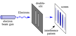
Double-slit experiment (redirect from Double-slit diffraction)
Fresnel diffraction equation, which implies that as the plane of observation gets closer to the plane in which the slits are located, the diffraction patterns...
79 KB (8,688 words) - 11:28, 26 June 2025
Anónima Desportiva, a type of incorporated sports club in Portugal Selected area diffraction, a crystallographic experimental technique Sum of absolute differences...
2 KB (231 words) - 23:47, 11 November 2024

projector lens (using an intermediate lens) produces a diffraction pattern (low-energy electron diffraction, LEED) at the imaging plane and recorded in a number...
24 KB (2,925 words) - 01:51, 24 June 2025

information within each diffraction pattern can be analysed in more detail. For texture and orientation measurements, the diffraction patterns are binned...
124 KB (13,688 words) - 12:35, 24 June 2025

the electrons then sharp diffraction features are normally observed, a technique called selected area electron diffraction. This is often the main technique...
48 KB (5,271 words) - 05:57, 20 June 2025

set so) to an instant update of the simulated diffraction pattern. If any diffraction spot is selected, corresponding crystallographic planes are shown...
36 KB (3,555 words) - 19:45, 11 November 2024

Convergent beam electron diffraction (CBED) is an electron diffraction technique where a convergent or divergent beam (conical electron beam) of electrons...
23 KB (2,702 words) - 12:42, 23 May 2025
used in semiconductor manufacturing Selected Area Diffraction Pattern, the pattern of spots in Selected area diffraction sADP, "slow after depolarizing current"...
658 bytes (115 words) - 16:39, 25 October 2019

strength of current to the intermediate lens, the diffraction pattern is projected on a screen. Diffraction is a very powerful tool for doing a cell reconstruction...
118 KB (15,040 words) - 22:02, 23 June 2025
4D scanning transmission electron microscopy (section Virtual Diffraction (Dark Field / Bright Field) Imaging)
scanning electron nano diffraction (SEND), nanobeam electron diffraction (NBED), or pixelated STEM. The use of diffraction patterns as a function of...
41 KB (4,825 words) - 02:05, 24 June 2025

of the incoming beam that is selecting the diffracted beam. The selective aperture selects the area where the diffraction comes from. The WBDF image is...
23 KB (3,483 words) - 22:13, 15 April 2025

oxides containing Cu, Zr, and W were believed to be created, selected area diffraction (SAD) of the ceramic product has proven the existence of Cu2O...
10 KB (1,053 words) - 20:52, 25 May 2025
tomography Seismological Society of America Selected-ion flow-tube mass spectrometry Selected area diffraction Selection rule Selective adsorption Selective...
32 KB (3,248 words) - 12:19, 30 July 2024

Electron Microscopy (HRTEM) and cell parameters calculated from Selected Area Diffraction (SAED). Infrared absorbance peaks of barium ferrate are observed...
10 KB (931 words) - 06:34, 26 November 2024

for instance by Community in their SQ 90 high-frequency horn. JBL's diffraction or "Smith" horn was a variation on the radial design, using a very small...
41 KB (4,563 words) - 06:24, 25 June 2025
transmission electron microscopy images, electron diffraction patterns including convergent-beam electron diffraction or combinations of these. It has been successful...
47 KB (4,958 words) - 03:17, 24 June 2025

Image sensor format (redirect from Sensor active area)
resolution of all optical systems is limited by diffraction. One way of considering the effect that diffraction has on cameras using different sized sensors...
57 KB (6,612 words) - 23:47, 13 May 2025
Rietveld refinement (category Diffraction)
transfer Q, which is historically rarely used in powder diffraction but very common in all other diffraction and optics techniques. The relation is Q = 4 π sin...
34 KB (5,596 words) - 08:26, 24 April 2025

Kikuchi lines (physics) (category Diffraction)
thick regions of either selected area or convergent beam electron diffraction patterns, but difficult to see in diffraction from crystals much less than...
17 KB (2,222 words) - 19:50, 19 January 2025

Birkbeck College in 1953. Franklin is best known for her work on the X-ray diffraction images of DNA while at King's College London, particularly Photo 51,...
167 KB (18,931 words) - 19:11, 14 June 2025

Optics (section Diffraction and optical resolution)
of situations such as diffraction through a single gap, diffraction through multiple slits, or diffraction through a diffraction grating that contains...
107 KB (12,886 words) - 21:46, 13 May 2025

landscape[clarification needed] diffraction into the "street canyon" below multipath reflection along the street diffraction through windows, and attenuated...
13 KB (1,804 words) - 02:02, 8 December 2024
broadly available. Electron diffraction to solve crystal structures date back to the earliest days of electron diffraction. The first successful demonstration...
20 KB (2,142 words) - 14:40, 23 May 2025
Magnetolithography Scanning probe lithography Surface-charge lithography Diffraction lithography These processes differ in speed and cost, as well as in the...
3 KB (347 words) - 00:21, 6 January 2025