
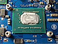
Haswell is the codename for a processor microarchitecture developed by Intel as the "fourth-generation core" successor to the Ivy Bridge (which is a die...
109 KB (4,974 words) - 13:06, 17 December 2024
Advanced Vector Extensions (redirect from Haswell New Instructions)
new instructions. They were first supported by Intel with the Haswell microarchitecture, which shipped in 2013. AVX-512 expands AVX to 512-bit support...
51 KB (4,089 words) - 23:38, 15 May 2025

It is Intel's codename for the 14 nanometer die shrink of its Haswell microarchitecture. It is a "tick" in Intel's tick–tock principle as the next step...
61 KB (3,087 words) - 12:36, 22 June 2025

Pentium (section Haswell microarchitecture based)
into older CPU sockets. In parallel with the P5 microarchitecture, Intel developed the P6 microarchitecture and started marketing it as the Pentium Pro for...
41 KB (2,656 words) - 23:31, 1 July 2025

LGA 1150 (section Haswell chipsets)
for CPUs built on the Haswell microarchitecture. This socket is also used by the Haswell's successor, Broadwell microarchitecture. It is the successor...
23 KB (1,168 words) - 21:36, 16 January 2025

integrated GPU is branded as "Intel Graphics" but still use the same GPU microarchitecture as "Intel Arc Graphics" on the H series models. All models support...
199 KB (13,736 words) - 13:00, 7 July 2025
of the Haswell Islands Haswell (surname) Haswell (microarchitecture), the Intel codename for a processor (CPU) microarchitecture 23809 Haswell, an asteroid...
732 bytes (113 words) - 12:34, 24 July 2018
Sandy Bridge, using 22 nm process, released in April 2012. Haswell 22 nm microarchitecture, released June 3, 2013. Added a number of new instructions...
52 KB (2,899 words) - 15:22, 17 July 2025
E5-26xx v3 processors, which belong to the Haswell-E and Haswell-EP variants of the Haswell microarchitecture, respectively. All supported processors use...
11 KB (1,115 words) - 15:31, 27 June 2024
Ivy Bridge microarchitecture included a "next-generation" implementation of Quick Sync. Version 3 (Haswell) The Haswell microarchitecture implementation...
24 KB (1,922 words) - 02:55, 23 July 2025
Xeon (redirect from Haswell-EP)
series based on the Haswell microarchitecture. It uses the new LGA 1150 socket, which was introduced with the desktop Core i5/i7 Haswell processors, incompatible...
116 KB (7,807 words) - 03:16, 22 July 2025

astronomy telescope near Haswell In 2013, the Intel corporation announced that it was naming its newest processor microarchitecture Haswell, after the town. Geography...
11 KB (847 words) - 01:49, 8 July 2025
Nehalem microarchitecture and LZCNT beginning with the Haswell microarchitecture. AMD implements both, beginning with the Barcelona microarchitecture. AMD...
23 KB (1,583 words) - 12:40, 4 July 2025

launched on August 5, 2015, succeeding the Broadwell microarchitecture. Skylake is a microarchitecture redesign using the same 14 nm manufacturing process...
100 KB (4,901 words) - 14:28, 18 June 2025
Ivy Bridge is the codename for Intel's 22 nm microarchitecture used in the third generation of the Intel Core processors (Core i7, i5, i3). Ivy Bridge...
65 KB (2,672 words) - 19:39, 9 June 2025
and in successive microarchitectures like Ivy Bridge and Haswell.: 121–123 AMD implemented a μop cache in their Zen microarchitecture. Fetching complete...
99 KB (13,735 words) - 12:24, 8 July 2025
Consumer Ultra-Low Voltage (CULV) is a computing platform developed by Intel. It was estimated in January 2009 that this market could reach 10 million...
42 KB (371 words) - 11:54, 4 April 2024

Sandy Bridge (redirect from Intel Sandy Bridge (microarchitecture))
Intel's 32 nm microarchitecture used in the second generation of the Intel Core processors (Core i7, i5, i3). The Sandy Bridge microarchitecture is the successor...
61 KB (2,688 words) - 19:44, 9 June 2025

capabilities were planned to be integrated in CPUs based on the Haswell microarchitecture. Larrabee's philosophy of using many small, simple cores was similar...
26 KB (2,916 words) - 22:25, 11 July 2025
referred to as BMI1) and BMI2; they were both introduced with the Haswell microarchitecture with BMI1 matching features offered by AMD's ABM instruction set...
19 KB (1,446 words) - 21:46, 26 July 2025
much as 50%, that were reported by Intel in their release of the Haswell microarchitecture; where they dropped their power consumption benchmark from 30–40...
27 KB (3,259 words) - 02:35, 27 July 2025
Intel Core (section Broadwell microarchitecture)
22 nm process technology and better graphics. Haswell is the fourth generation Core processor microarchitecture, and was released in 2013. Broadwell is the...
276 KB (9,952 words) - 07:00, 28 July 2025

Bridge Microarchitecture: Memory Subsystem". realworldtech.com. Retrieved December 8, 2014. David Kanter (November 13, 2012). "Intel's Haswell CPU Microarchitecture:...
6 KB (552 words) - 05:59, 18 July 2025
June 2013 on selected Intel microprocessors based on the Haswell microarchitecture. Haswell processors below 45xx as well as R-series and K-series (with...
27 KB (2,487 words) - 10:57, 19 March 2025
List of Intel Core processors (section Haswell-DT)
original Core (Solo/Duo) mobile series based on the Enhanced Pentium M microarchitecture, as well as its Core 2- (Solo/Duo/Quad/Extreme), Core i3-, Core i5-...
497 KB (14,119 words) - 09:55, 18 July 2025

generation Ultrabook specification, introduced in June 2013 alongside its new Haswell processor architecture, Intel also added the requirement for all future...
22 KB (1,365 words) - 06:13, 10 January 2025

architectures gain required hardware support; for example, since the Haswell microarchitecture (announced in 2013), Intel started to include VMCS shadowing as...
32 KB (3,512 words) - 22:56, 1 June 2025
FDI, see Westmere (microarchitecture), Sandy Bridge (microarchitecture), Ivy Bridge (microarchitecture), Haswell (microarchitecture). Most of them are...
3 KB (372 words) - 15:27, 23 April 2024
Kanter, David (2010-09-25). "Intel's Sandy Bridge Microarchitecture". "The Haswell Front End - Intel's Haswell Architecture Analyzed: Building a New PC and...
37 KB (4,261 words) - 15:21, 26 July 2025

to 92% power efficiency. Due to the integration of the Intel Haswell microarchitecture and Microsoft officially ending support for the Windows XP operating...
44 KB (4,706 words) - 19:56, 12 June 2025