
Multi-project chip (MPC), and multi-project wafer (MPW) semiconductor manufacturing arrangements allow customers to share tooling (like mask) and microelectronics...
19 KB (2,030 words) - 08:36, 4 April 2025
Implementation Service) is multi-project wafer service that provides metal–oxide–semiconductor (MOS) chip design tools and related services that enable universities...
5 KB (429 words) - 00:41, 25 February 2025

manufacturer. Some manufacturers and IC design houses offer multi-project wafer service (MPW) as a method of obtaining low cost prototypes. Often called...
26 KB (3,098 words) - 13:40, 8 May 2025
subcontract mask making, wafer manufacturing, dicing and packaging to vendors; final testing to get prototype samples Multi-project wafer service Integrates multiple...
3 KB (221 words) - 06:48, 11 March 2025
WaferCatalyst is a Multi-Project Wafer (MPW) consolidation service by King Abdulaziz City for Science and Technology (KACST), Saudi Arabia. WaferCatalyst...
2 KB (302 words) - 20:19, 17 January 2025
Shuttle (redirect from Shuttle service)
transportation Multi-project wafer service (|MPW) shuttle, an integrated circuit production run for multi-chip or multi-project wafers Shuttle bombing...
3 KB (498 words) - 05:29, 20 October 2024
knowledge base Millilumen (mlm), a unit of luminous flux Multi-layer mask, in multi-project wafer service in semiconductor fabrication Multipurpose Laboratory...
866 bytes (135 words) - 01:23, 21 November 2024
design services, and others, like Samsung, design and manufacture ICs for customers, while also designing, manufacturing and selling their own ICs. Wafer size...
208 KB (6,860 words) - 23:03, 6 May 2025

on Computer-Aided Design of Integrated Circuits and Systems Multi-project wafer service Standard cell Parker Brakus (May 17, 2022). "Analog IC: Understanding...
27 KB (3,437 words) - 06:05, 16 April 2025

Pro Wrestling, a Lucha libre professional wrestling promotion Multi-project wafer service, integrated circuit production that includes designs from various...
818 bytes (125 words) - 23:16, 28 December 2020
DARPA (redirect from Defense Advanced Research Project Agency)
mechanical beam-steering, detectors, electronics) in a single device. Create a wafer-scale system that is one hundred times smaller and lighter than existing...
135 KB (12,488 words) - 03:24, 5 May 2025

Nvidia (redirect from Project GROOT)
Nvidia uses external suppliers for all phases of manufacturing, including wafer fabrication, assembly, testing, and packaging. Nvidia thus avoids most of...
159 KB (13,656 words) - 20:07, 8 May 2025
A multi-user dungeon (MUD, /mʌd/), also known as a multi-user dimension or multi-user domain, is a multiplayer real-time virtual world, usually text-based...
82 KB (9,177 words) - 00:24, 2 May 2025

Johnson 2002, p. 203. Wafer 1991, p. 116. Wafer 1991, p. 16. Wafer 1991, p. 198. Wafer 1991, pp. 124, 198. Wafer 1991, p. 14. Wafer 1991, pp. 14, 198; Hayes...
93 KB (12,463 words) - 11:33, 29 April 2025

Polycrystalline silicon (redirect from Wafer-based silicon)
grow single crystal boules. The boules are then sliced into thin silicon wafers and used for the production of solar cells, integrated circuits and other...
41 KB (4,485 words) - 21:05, 5 April 2025
milestone that followed was the Multi Project Chip (MPC) concept that allowed multiple designs to be fabricated on a single wafer, greatly reducing cost to...
7 KB (769 words) - 10:41, 14 December 2024
October 31, Google announced they would sponsor no-cost OpenMPW (multi-project wafer) shuttle runs for it in the coming months. GlobalFoundries was a...
82 KB (5,392 words) - 21:16, 21 April 2025

List of megaprojects in India (redirect from Indian mega project)
develop Rs 1,770 crore Multi Modal Logistics Park in Bengaluru". 19 September 2023. "Rajkot: 33-year-long wait over, Girnar ropeway project gets green nod"....
145 KB (3,690 words) - 17:44, 20 April 2025

A stepper or wafer stepper is a device used in the manufacture of integrated circuits (ICs). It is an essential part of the process of photolithography...
23 KB (3,204 words) - 04:36, 22 January 2025
been changed to multi-colour. Note: the blood-red drips behind the letters of the title have returned, after having been changed to multi-colour for two...
157 KB (321 words) - 00:02, 27 March 2025

use multi-gate FinFET or GAAFET transistors instead of planar ones, starting at the 22 nm node (Intel) or 16/14 nm nodes. Mono-crystal silicon wafers are...
86 KB (9,193 words) - 03:50, 27 April 2025
SunEdison (category Silicon wafer producers)
silicon ingots, silicon wafers, solar modules, solar energy systems, and solar module racking systems. Originally a silicon-wafer manufacturer established...
44 KB (4,146 words) - 00:46, 14 September 2024

PerkinElmer (section Hubble optics project)
single small mask to be stepped across the wafer, rather than requiring a single large mask covering the entire wafer. The company never regained their lead...
32 KB (3,314 words) - 15:35, 23 March 2025

CHIPS and Science Act (section Project announcements)
fiscal years 2025-27, outlining goals that range from scaling up multi-process wafer access to computer-aided design of chips to organizing the Workforce...
137 KB (13,104 words) - 12:58, 2 May 2025
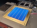
Heterojunction solar cell (section Multi-junction)
resistance; bulk carrier lifetimes; the saturation current density; wafer resistivity and wafer thickness. These factors in turn affect the V O C {\displaystyle...
131 KB (13,981 words) - 22:08, 11 February 2025

wine reduction, and a communion wafer. A local Catholic food blogger acknowledged that while the unconsecrated wafer is not the Eucharist, it is still...
160 KB (12,357 words) - 01:42, 9 May 2025
is based on FinFET (fin field-effect transistor) technology, a type of multi-gate MOSFET technology. As of 2021, the IRDS Lithography standard gives...
50 KB (4,709 words) - 20:23, 20 April 2025

Singapore (category Pages using Sister project links with hidden wikidata)
English is the common language, with exclusive use in numerous public services. Multi-racialism is enshrined in the constitution and continues to shape national...
327 KB (27,743 words) - 01:10, 7 May 2025

release, the yield for the new chip was zero. That is, for every wafer sent through the multi-step process, zero working chips would be produced. Gary Johnson...
28 KB (2,925 words) - 23:53, 27 February 2025