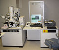
Maskless lithography (MPL) is a photomask-less photolithography-like technology used to project or focal-spot write the image pattern onto a chemical resist-coated...
16 KB (1,995 words) - 15:31, 27 May 2025
Photolithography (redirect from Optical lithography)
"MAPPER: High Throughput Maskless Lithography". January 2009. pp. 1–5. Weiland, Marco. "MAPPER: High throughput Maskless Lithography" (PDF). cea.fr. "Manufacturing...
59 KB (6,439 words) - 19:14, 23 May 2025
electron-beam lithography is that it can draw custom patterns (direct-write) with sub-10 nm resolution. This form of maskless lithography has high resolution...
38 KB (4,736 words) - 02:29, 26 May 2025
oven, and later the pattern is defined on the photoresist using maskless lithography with an electron beam. This step is called exposure. The exposed...
124 KB (14,509 words) - 06:16, 23 May 2025
momentum charged particles with very great precision. E-beam lithography Maskless lithography Nanochannel glass materials Photolithography F. Watt∗, A. A...
4 KB (503 words) - 09:17, 28 May 2024
MEMS (section Lithography)
beam lithography is that it is one of the ways to beat the diffraction limit of light and make features in the nanometer range. This form of maskless lithography...
45 KB (5,603 words) - 20:43, 20 March 2025
Photomask (category Lithography (microfabrication))
have since been replaced by electron beam lithography and laser-driven mask writer or maskless lithography systems which generate reticles directly from...
20 KB (2,321 words) - 02:03, 25 May 2025
are primarily marketed for image projection, displays devices, and maskless lithography.[citation needed] SLMs are also used in optical computing and holographic...
11 KB (1,201 words) - 11:51, 1 January 2025
Plasmonic nanolithography (redirect from Plasmonic lithography)
coupling. Plasmonic direct writing is a maskless form of photolithography that is based on scanning probe lithography; the method uses localized surface plasmon...
13 KB (1,223 words) - 11:11, 15 March 2025
Knoll, Armin W.; Duerig, Urs (September 11, 2013). "Thermal Probe Maskless Lithography for 27.5 nm Half-Pitch Si Technology". Nano Letters. 13 (9): 4485–4491...
17 KB (1,822 words) - 04:39, 20 August 2024
to film photograph. The main alternative to using phototools is maskless lithography, more commonly referred to as direct imaging. Chemistry of Photography...
1 KB (120 words) - 19:41, 30 December 2024
Dip-pen nanolithography (category Lithography (microfabrication))
ISSN 1613-6810. PMID 17294474. Maskless lithography Nature Chemistry Vol 1, August 2009 Woo, Dai, King & Sheehan "Maskless Nanoscale Writing of Nanoparticle-Polymer...
22 KB (2,562 words) - 06:44, 25 May 2025
Scanning probe lithography (SPL) describes a set of nanolithographic methods to pattern material on the nanoscale using scanning probes. It is a direct-write...
23 KB (2,368 words) - 07:29, 25 November 2024
Nanolithography (category Lithography (microfabrication))
sub-10 nm resolutions have been achieved. This form of direct-write, maskless lithography has high resolution and low throughput, limiting single-column e-beams...
15 KB (1,679 words) - 19:00, 15 May 2025
Electron-beam technology (section Lithography)
is also used to produce computer-generated holograms (CGH). Maskless electron lithography has found wide usage in photomask making for photolithography...
11 KB (1,403 words) - 11:46, 25 May 2025
resist. A laser may be used instead of a photomask. This is known as maskless lithography or direct imaging. PCB milling uses a two or three-axis mechanical...
35 KB (4,567 words) - 01:10, 7 March 2025
Trade and Industry) CEA-Leti and Nokia Research Center IMAGINE, maskless lithography CEA-Leti's European partnerships are aimed at strengthening Europe's...
10 KB (1,117 words) - 20:24, 27 April 2025
W.; Park, H.; Yu, K.; Park, N.; & Kwon, S. (2007). Optofluidic maskless lithography system for real-time synthesis of photopolymerized microstructures...
16 KB (1,847 words) - 06:06, 23 May 2025
Brad; Linn, Allison; Joy, David C.; Rondinone, Adam J. (2015). "Maskless Lithography and in situ Visualization of Conductivity of Graphene using Helium...
5 KB (485 words) - 13:50, 25 April 2025
developed miniature, all-electrostatic columns for e-beam lithography, that provide a maskless and high throughput platform for writing nanoscale IC patterns...
7 KB (600 words) - 18:19, 30 January 2025
ion implantation, optical lithography, and reactive ion etching. E-beam lithography Ion beam lithography Maskless lithography Nanolithography Photolithography...
6 KB (611 words) - 23:48, 23 April 2025
Alvéole Lab (category Lithography (microfabrication))
microenvironment in vitro. Its first product is Primo, a contactless and maskless photopatterning device allowing researchers to control the topography (via...
7 KB (649 words) - 11:07, 12 February 2023
doi:10.1116/1.588626. Basu, A. S.; et al. (2004). "Scanning thermal lithography: Maskless, submicron thermochemical patterning of photoresist by ultracompliant...
11 KB (1,240 words) - 16:41, 4 May 2025
"Diffractive optical variable image devices generated by maskless interferometric lithography for optical security". In Costa, Manuel F (ed.). International...
10 KB (1,127 words) - 23:07, 13 November 2024
should not be confused with using a beam of focused ions for direct write lithography (such as in proton beam writing). These are generally quite different...
26 KB (3,261 words) - 23:21, 18 April 2025
Xiong, S.; Rho, J.; Sun, C.; Bogy, D. B.; Zhang, X. (2011). "Maskless Plasmonic Lithography at 22 nm Resolution". Scientific Reports. 1: 175. Bibcode:2011NatSR...
24 KB (2,705 words) - 02:27, 25 May 2025
patterns on material, such as screen printing, flexography, gravure, offset lithography, and inkjet. By electronic-industry standards, these are low-cost processes...
49 KB (5,431 words) - 17:53, 23 May 2025


