
Electron-beam lithography (often abbreviated as e-beam lithography or EBL) is the practice of scanning a focused beam of electrons to draw custom shapes...
38 KB (4,735 words) - 04:01, 12 May 2024
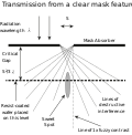
Photolithography (redirect from Optical lithography)
as electron beam lithography, X-ray lithography, extreme ultraviolet lithography and ion projection lithography. Extreme ultraviolet lithography has...
57 KB (6,366 words) - 21:27, 3 May 2024
used form of maskless lithography today is electron beam lithography. Its widespread use is due to the wide range of electron beam systems available accessing...
16 KB (1,991 words) - 03:23, 16 May 2024
prints. X-rays generate secondary electrons as in the cases of extreme ultraviolet lithography and electron beam lithography. While the fine pattern definition...
12 KB (1,623 words) - 17:49, 28 December 2022
compared to x-ray and e-beam lithography. Ion-beam lithography, or ion-projection lithography, is similar to Electron beam lithography, but uses much heavier...
4 KB (503 words) - 00:22, 8 December 2021
Nanolithography (category Lithography (microfabrication))
20 nm resolution. Electron beam lithography (EBL) or electron-beam direct-write lithography (EBDW) scans a focused beam of electrons on a surface covered...
16 KB (1,682 words) - 05:37, 13 May 2024
any lithography method which uses a shorter-wavelength light or beam type than the current state of the art, such as X-ray lithography, electron beam lithography...
10 KB (1,111 words) - 00:58, 10 January 2024
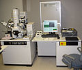
Etec Systems (section Electron beam lithography tools)
an American producer of scanning electron microscopes, electron beam lithography tools, and laser beam lithography tools from 1970 until 2005. It was...
5 KB (485 words) - 22:04, 15 January 2022
The proximity effect in electron beam lithography (EBL) is the phenomenon that the exposure dose distribution, and hence the developed pattern, is wider...
4 KB (598 words) - 19:02, 11 December 2022

an oven, and later exposed to laser light, using maskless lithography with an electron beam. The exposed photoresist is developed (removed) and the unprotected...
137 KB (15,597 words) - 18:02, 15 May 2024

MEMS (section Lithography)
acts as a lens. Electron beam lithography (often abbreviated as e-beam lithography) is the practice of scanning a beam of electrons in a patterned fashion...
45 KB (5,625 words) - 01:38, 16 May 2024
Cathode ray (redirect from Electron beam)
Cathode rays or electron beams (e-beam) are streams of electrons observed in discharge tubes. If an evacuated glass tube is equipped with two electrodes...
19 KB (2,648 words) - 03:54, 12 May 2024

materials that would otherwise be considered unsuitable for welding. Electron-beam lithography (EBL) is a method of etching semiconductors at resolutions smaller...
152 KB (15,321 words) - 18:16, 14 May 2024
cable-isolation treatment, in electron lithography of sub-micrometer and nano-dimensional images, in microelectronics for electron-beam curing of color printing and...
9 KB (1,177 words) - 16:23, 2 August 2023
Security hologram (section Electron-beam lithography)
holograms are created using highly sophisticated and very expensive electron-beam lithography systems. This kind of technology allows the creation of surface...
9 KB (1,194 words) - 01:35, 19 March 2024
biotechnology. Electron interference lithography may be used for patterns which normally take too long for conventional electron beam lithography to generate...
11 KB (1,350 words) - 23:44, 3 December 2023

over other forms of lithography (such as photolithography and electron beam lithography). They include the following: Lower cost than traditional photolithography...
4 KB (368 words) - 21:30, 13 February 2024

Photoresist (category Lithography (microfabrication))
photoresists for electron-beam exposure. Electron beam lithography usually relies on resists dedicated specifically to electron-beam exposure. Physical...
29 KB (3,241 words) - 22:08, 18 May 2024

Polydimethylsiloxane (section Soft lithography)
is produced from the normal techniques of photolithography or electron-beam lithography. The resolution depends on the mask used and can reach 6 nm. The...
38 KB (4,221 words) - 14:25, 26 April 2024
either of the beams. FIB should not be confused with using a beam of focused ions for direct write lithography (such as in proton beam writing). These...
26 KB (3,322 words) - 22:07, 2 March 2024
Microlithography (category Lithography (microfabrication))
Electron beam lithography, using a steerable electron beam. Nanoimprinting Interference lithography Magnetolithography Scanning probe lithography Surface-charge...
3 KB (347 words) - 23:57, 18 July 2023

Vacuum tube (redirect from Electron valve)
create a beam of electrons for display purposes (such as the television picture tube, in electron microscopy, and in electron beam lithography); X-ray...
119 KB (15,311 words) - 22:22, 14 May 2024
Corporation (Santa Clara, CA), which manufactures complementary electron beam lithography (CEBL) systems. He also heads the David Lam Group, an investor...
15 KB (1,542 words) - 08:41, 18 January 2024
optical lithography, X-ray lithography, dip pen nanolithography, electron beam lithography or nanoimprint lithography were also developed. Lithography is a...
78 KB (8,283 words) - 15:00, 9 April 2024

Scanning tunneling microscope (redirect from Electron tunnel microscopy)
also use the STM to tunnel electrons into a layer of electron-beam photoresist on the sample, in order to do lithography. This has the advantage of offering...
47 KB (7,075 words) - 21:04, 29 April 2024

the National Academy of Engineering for contributions to electronic beam lithography and microscopy and for leadership in microfabrication. Broers was born...
23 KB (2,370 words) - 01:57, 10 May 2024

Multiple patterning (category Lithography (microfabrication))
line-cutting at its 45nm node or TSMC at its 28nm node. Even for electron-beam lithography, single exposure appears insufficient at ~10 nm half-pitch, hence...
65 KB (7,206 words) - 15:06, 18 May 2024
Electron-beam-induced deposition (EBID) is a process of decomposing gaseous molecules by an electron beam leading to deposition of non-volatile fragments...
12 KB (1,419 words) - 20:16, 10 December 2023
resistance of a conductor Proximity effect (electron beam lithography), a phenomenon in electron beam lithography (EBL) Proximity effect (superconductivity)...
917 bytes (130 words) - 06:36, 24 April 2018
microscopes and other electron beam instruments (such as those used for electron beam lithography), it is helpful to start with an electron source that is small...
125 KB (16,087 words) - 09:14, 8 February 2024