 | A p–n junction is a combination of two types of semiconductor materials, p-type and n-type, in a single crystal. The "n" (negative) side contains freely-moving... 19 KB (2,740 words) - 01:19, 5 May 2024 |
 | BJTs use two p–n junctions between two semiconductor types, n-type and p-type, which are regions in a single crystal of material. The junctions can be made... 55 KB (6,795 words) - 21:00, 28 April 2024 |
p–n junction isolation is a method used to electrically isolate electronic components, such as transistors, on an integrated circuit (IC) by surrounding... 5 KB (577 words) - 20:59, 17 March 2023 |
of p–n diode behavior than is found in the articles p–n junction or diode. A p–n diode is a type of semiconductor diode based upon the p–n junction. The... 24 KB (3,637 words) - 15:12, 17 March 2024 |
Depletion region (redirect from Junction voltage) depletion region forms instantaneously across a p–n junction. It is most easily described when the junction is in thermal equilibrium or in a steady state:... 17 KB (2,559 words) - 01:39, 24 March 2024 |
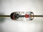 | Diode (redirect from Junction diode) type today, is a crystalline piece of semiconductor material with a p–n junction connected to two electrical terminals. It has an exponential current–voltage... 63 KB (7,334 words) - 02:27, 27 March 2024 |
PIN diode (redirect from P-i-n junction) structure, or p-i-n junction, of a solar cell. In this case, the advantage of using a PIN structure over conventional semiconductor p–n junction is better... 15 KB (2,178 words) - 21:45, 14 January 2024 |
contact. Electrical junctions types include thermoelectricity junctions, metal–semiconductor junctions and p–n junctions. Junctions are either rectifying... 1 KB (133 words) - 17:43, 22 October 2023 |
a p-n junction diode, electrons and holes are the minority charge carriers in the p-region and the n-region, respectively. In an unbiased junction, due... 5 KB (723 words) - 20:54, 28 January 2023 |
Quasi Fermi level (section p-n junction) applied to a p-n junction, the quasi Fermi levels for electron and holes overlap with one another. As bias increase, the valence band of the p-side gets... 6 KB (1,059 words) - 20:50, 15 November 2021 |
Ohmic contact (redirect from Nonrectifying junction) a junction or contact that does not demonstrate a linear I–V curve is called non-ohmic. Non-ohmic contacts come in a number of forms, such as p–n junction... 13 KB (1,470 words) - 22:14, 28 December 2022 |
to electrically isolate components on a semiconductor crystal, using p–n junction isolation. The first monolithic IC chip was invented by Robert Noyce... 74 KB (9,046 words) - 22:20, 4 April 2024 |
 | example, and particularly, the p–n junction—will receive this energy, and because of the asymmetric response of the junction to an electric field, it will... 5 KB (540 words) - 22:30, 14 January 2024 |
concentration and regions of p- and n-type dopants. A single semiconductor device crystal can have many p- and n-type regions; the p–n junctions between these regions... 46 KB (5,377 words) - 04:54, 29 April 2024 |
 | Theory of solar cells (section The p-n junction) (the n-type side of the junction) into the region of low electron concentration (p-type side of the junction). When the electrons diffuse into the p-type... 32 KB (4,674 words) - 06:13, 27 April 2024 |
 | p–n junction with a low Zener voltage, in which case the reverse conduction occurs due to electron quantum tunnelling in the short distance between p... 18 KB (2,326 words) - 18:34, 1 April 2024 |
 | cells are composed of p-type and n-type semiconductor layers sandwiched together, forming the source of built-in voltage (a p-n junction). Due to differing... 7 KB (905 words) - 15:47, 1 December 2023 |
most common semiconductor device today, is known as a p–n junction.) Metal–semiconductor junctions are crucial to the operation of all semiconductor devices... 19 KB (2,205 words) - 23:21, 12 February 2024 |
 | its internal junction and diffusion capacitance and reverse recovery time. Shockley derives an equation for the voltage across a p-n junction in a long article... 12 KB (1,831 words) - 22:29, 3 January 2024 |
 | JFET (redirect from Junction Field-Effect Transistor) holes (p-type), or of negative carriers or electrons (n-type). Ohmic contacts at each end form the source (S) and the drain (D). A pn-junction is formed... 20 KB (2,415 words) - 16:11, 31 March 2024 |
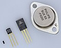
| Transistor (section Bipolar junction transistor (BJT)) two p-type semiconductors (a p–n–p transistor). This construction produces two p–n junctions: a base-emitter junction and a base-collector junction, separated... 95 KB (9,876 words) - 02:40, 24 April 2024 |
 | Multi-junction (MJ) solar cells are solar cells with multiple p–n junctions made of different semiconductor materials. Each material's p-n junction will... 61 KB (8,207 words) - 17:49, 19 April 2024 |
 | creating a p-type semiconductor. Joining n-type silicon to p-type silicon creates a p–n junction with a common Fermi level; electrons flow from n to p, while... 85 KB (10,618 words) - 11:20, 10 May 2024 |
are also critical to a full analysis of p-n junction devices such as bipolar junction transistors and p-n junction diodes. The electron–hole pair is the... 27 KB (4,197 words) - 22:39, 7 March 2024 |
 | positive-to-negative (P-N) junction that is about 10 nm (100 Å) wide. The heavy doping results in a broken band gap, where conduction band electron states on the N-side... 14 KB (1,472 words) - 06:23, 17 April 2024 |
Method measurements yield a 70% drop. Safe operating area P-N Junction Metal Semiconductor Junction Sabatier, Jocelyn (2015-05-06). Fractional Order Differentiation... 6 KB (716 words) - 19:32, 5 February 2024 |
 | Doping (semiconductor) (redirect from P-doping) the p-n junction's properties are due to the band bending that happens as a result of the necessity to line up the bands in contacting regions of p-type... 35 KB (4,525 words) - 15:14, 6 March 2024 |
device similar to a JFET with a Schottky (metal–semiconductor) junction instead of a p–n junction for a gate. MESFETs are constructed in compound semiconductor... 4 KB (457 words) - 23:46, 9 August 2023 |
semiconductor devices. For example, the current near the depletion region of a p–n junction is dominated by the diffusion current. Inside the depletion region, both... 11 KB (1,420 words) - 08:28, 28 February 2024 |
 | photocells to gamma ray spectrometers. A photodiode is a PIN structure or p–n junction. When a photon of sufficient energy strikes the diode, it creates an... 29 KB (3,390 words) - 14:55, 7 May 2024 |